4 functional description, 1 block diagram, Figure 1: block diagram – Sundance SMT351T User Manual
Page 9: Fpga
SMT351T User Guide
Last Edited: 04/09/2009 11:26:00
4 Functional Description
The SMT351T provides a Virtex 5 FPGA, memory and IO connectors to allow the
development of applications ranging from Software defined Radio to MIMO, video,
Signal processing.
Typically, an ADC/DAC mezzanine can be fitted on the SLB connector and memory is
used to store burst data between the outside world/host/other TIMs, while the FPGA
implements functions on that data.
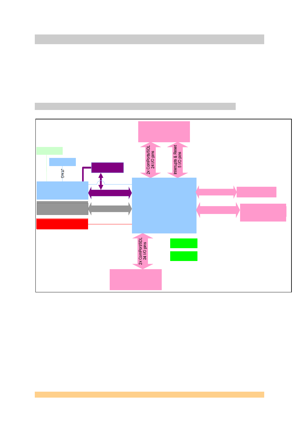
4.1 Block Diagram
Figure 1: Block Diagram
FPGA
Virtex-5 FF1136
XC5V
SX50T/LX50T/
SX95T/LX110T
1.0V Core
1.8V/2.5V/3.3V I/O
Xilinx Coolrunner II CPLD
XC2C256CP132 on
Comport3 and
Config&control
JTAG Header
J1 Top Primary TIM
Connector
ComPort/SDL 0 & 3
J2 Bottom Secondary TIM
Connector
ComPort/SDL 1 & 4
4 LEDs
JTAG
204 I/O pins
2 banks of
DDR2SDRAM
2x (64Mx16 or 128Mx16)
11 I/O pins
20 differential pairs
40 TTL IOs
Sundance Low-voltage Bus
(1 Conn.)
RSL clock
Flash memory
Local clock
ONLY with
LX160
16 RocketIO links
Sundance Rocket io
Serial Link (4 Conn.)
Switch