Figure 7 – Measurement Computing USB-7202 User Manual
Page 16
USB-7202 User's Guide
Functional Details
16
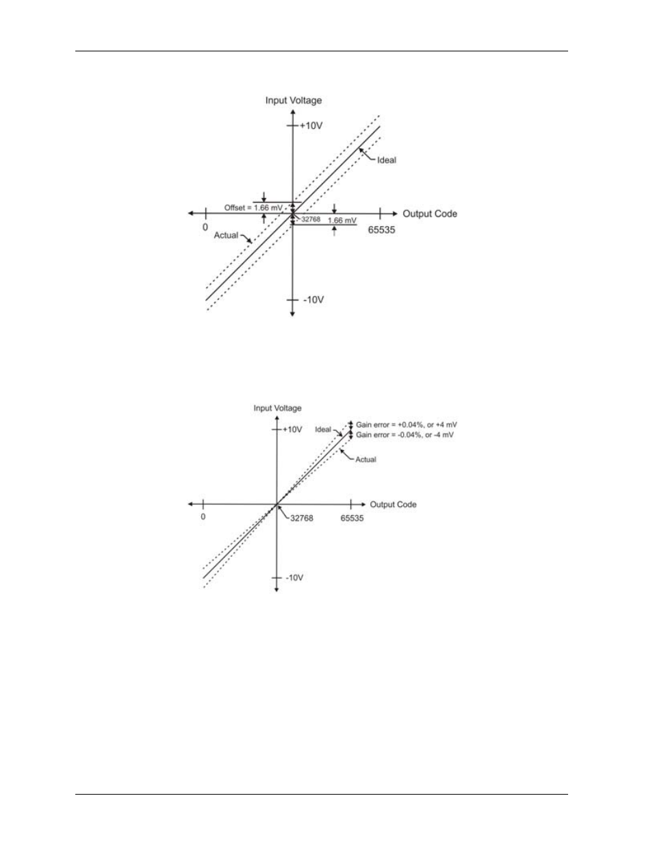
The accuracy plots in Figure 7 are drawn for clarity and are not drawn to scale.
Figure 7. ADC transfer function with offset error
Gain error is a change in the slope of the transfer function from the ideal, and is typically expressed as a
percentage of full-scale. Figure 8 shows the USB-7202 transfer function with gain error. Gain error is easily
converted to voltage by multiplying the full-scale input (±10 V) by the error.
The accuracy plots in Figure 8 are drawn for clarity and are not drawn to scale.
Figure 8. ADC Transfer function with gain error
For example, the USB-7202 exhibits a typical calibrated gain error of ±0.04% on all ranges. For the ±10 V
range, this would yield 10 V × ±0.0002 = ±4 mV. This means that at full scale, neglecting the effect of offset
for the moment, the measurement would be within 4 mV of the actual value. Note that gain error is expressed
as a ratio. Values near ±FS (±10 V) are more affected from an absolute voltage standpoint than are values
near mid-scale, which see little or no voltage error.
Combining these two error sources in Figure 9, we have a plot of the error band of the USB-7202 at ±full
scale (±10 V). This plot is a graphical version of the typical accuracy specification of the product.