Accuracy, Temperature – Measurement Computing PCI-DAS4020/12 User Manual
Page 23
PCI-DAS4020/12 User's Guide
Specifications
23
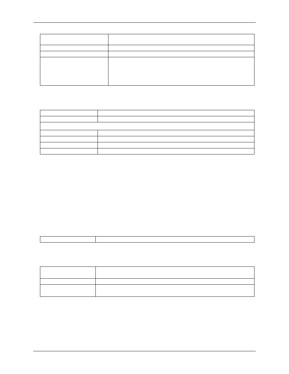
Data transfer
Via dual 32 K x 24 sample FIFO, SRAM based, with Bus-Master DMA and
scatter-gather, interrupt, or software polled.
A/D Conversion time
40 ns
Sample rate
20 MHz max, 1 kHz min
Throughput
Single channel: 20 MHz continuous
Two channels (0 and 1 or 2 and 3): 20 MHz continuous
Four channels:
10 MHz continuous
In background mode, the maximum throughput may be impacted by bus or
interrupt activity.
Accuracy
Table 3. Analog input accuracy specifications
Absolute accuracy
±5.5 LSB worst case error (either range)
Typical accuracy
±3.0 LSB error (either range)
Accuracy components:
Gain error
±2.0 LSB max, ±1.0 LSB typ
Offset error
±1.5 LSB max, ±1.0 LSB typ
Integral linearity error
±2.5 LSB max, ±1.0 LSB typ
Differential linearity error
±1.0 LSB max , ±0.4 LSB typ (No missing codes guaranteed)
Board error is a combination of gain, offset, integral linearity, and differential linearity error. The overall
absolute worst-case error of the board may be calculated by summing these component errors. Worst case error
is realized only in the unlikely event that each of the component errors are both at their maximum level, and
causing error in the same direction. Though this is very uncommon, it is still possible, and the calculated worst
case error of the PCI-DAS4020/12 board is ±7.0 LSB.
Each PCI-DAS4020/12 board is tested at the factory to make sure that its actual worst case error is less than
±5.0 LSB. Allowing for a 10% guard-band, the absolute worst-case error of a board is ±5.5 LSB. Typical
accuracy can be calculated from the various component typical errors in a similar fashion. This typical
maximum error calculation for the PCI-DAS4020/12 board yields ±3.4 LSB. However, this again assumes that
each of the errors is forcing an error in the same direction. Empirical evidence supports a conservative typical
error budget of ±3.0 LSB.
Table 4. Calibration specifications
Calibration
Auto-calibration. Calibration factors for each range stored on board in non-volatile RAM
Temperature
Table 5. Temperature specifications
Gain drift
±5 V range: ±0.10 LSB/°C max
±1 V range: ±0.13 LSB/°C max
Offset drift
±0.11 LSB/°C max, all ranges
Overall board temperature
drift
±5 V range: ±0.21 LSB/°C max
±1 V range: ±0.24 LSB/°C max
Overall, worst-case temperature drift is calculated by adding the drifts corresponding to the gain and offset
drifts. This worst case number is unlikely to occur, as it requires both gain and offset drifts to be at their
maximum levels, and to be affecting the measurement in the same direction. However, the overall board D/A
drift specifications have been calculated in this fashion.