Analog output, Digital i/o, Power distribution – Measurement Computing PCI-DAS4020/12 User Manual
Page 18: Input impedance configuration
PCI-DAS4020/12 User's Guide
Functional Details
18
Analog output
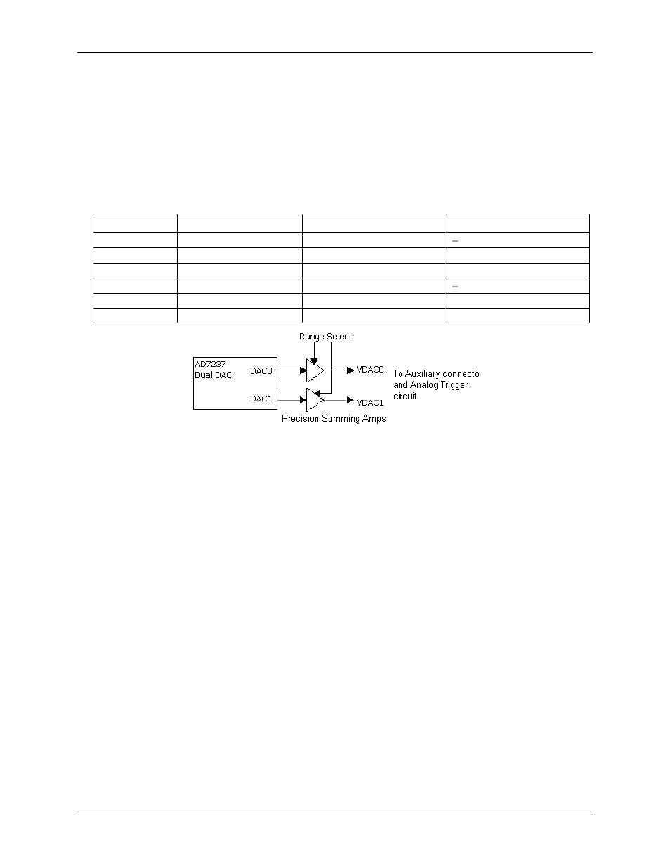
Two 12-bit voltage outputs are software programmable for ±10 V or ±5 V. The D/A is the Analog Devices
AD7237 Dual DAC. Since the DAC is dual buffered, the DAC output voltage is updated after the MS nibble is
written to the DAC.
The DACs initially power-up and are reset to 0 V. There is no calibration on these DACs. The offset and gain
errors are minimized by using precision components. The following table shows the DAC input coding.
DAC input coding
DAC Range
Input Code Binary
12 bit Input Code Hex
12 bit Output Voltage
± 10 V
0000 0000 0000
000h
10.000 V
± 10 V
1000 0000 0000
800h
0 V
± 10 V
1111 1111 1111
FFFh
+9.99513 V
± 5 V
0000 0000 0000
000h
5.000 V
± 5 V
1000 0000 0000
800h
0 V
± 5 V
1111 1111 1111
FFFh
+4.99756 V
Figure 9. Analog output block diagram
Digital I/O
The digital I/O is an 82C55 digital logic device. An external interrupt source pin (pin 1) and external interrupt
enable pin (pin 3) on the auxiliary 40-pin connector (
P3
) are used for external interrupts. These lines are pulled
up and an OR operation is performed on them to generate the external interrupt signal. Both are active low.
Power distribution
The PCI-DAS4020/12 board is powered by the PCI bus. The only power used is +5 V.
Input impedance configuration
Each analog input and the trigger/clock input channel on the PCI-DAS4020/12 has a dedicated solder gap. A
solder gap consists of two copper pads that you can solder together to change the input impedance of the
channel. When the solder gaps are open (default), the input impedance is 1.5 MΩ. When the solder gaps are
closed, the input impedance is 50 Ω.
To close the solder gaps and change the impedance to 50 ohm, solder the two copper pads together. To close the
solder gap, touch a soldering iron to the two contacts until some rosin core solder flows across the copper pads
and forms a small blob of solder. Be careful not to overheat the pads, or they may delaminate from the circuit
board. Do not add too much solder, as it could flow onto other components and cause an electrical short or other
defect.