Functional details, Pci-das4020/12 block diagram, Analog input signal path – Measurement Computing PCI-DAS4020/12 User Manual
Page 17: Chapter 3
17
Chapter 3
Functional Details
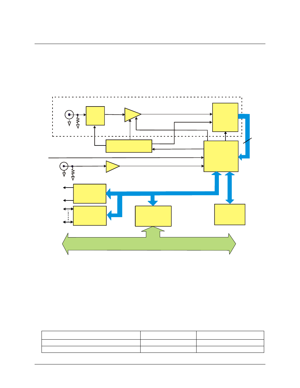
PCI-DAS4020/12 block diagram
PCI-DAS4020/12 functions are illustrated in the block diagram shown here.
BNC
BNC
Input
MUX
Gain & Offset
AUTOCAL
ADC
IN
System
Timing
Controller
Dual
32K x 24
SRAM
PC Bus
Controller
Dual12-bit
DAC
Digital I/0
(82C55)
PCI Bus Connector
(5V, 32 BIT, 33 MHZ)
VREF
CONV
Attenuator/
Amplifier
Analog
Clock/
Trigger
Local Bus
External Pacer
TRIG1, TRIG2,
or GATE
Four analog input channels per board
50 Ohm
Analog
Outputs
24 I/O
Four
Channels
12
S
Figure 8. PCI-DAS4020/12 functional block diagram
Analog input signal path
Four single-ended analog input channels, connect from BNC connectors to individual amplifiers and then
connect to dedicated ADC’s. Each path allows for:
50 ohm or high-Z termination, selected by solder gap
±1 V or ±5 V bipolar ranges, software-selectable (refer to the table below)
Auto-calibration for offset and gain adjustments for each channel and each range
Input range
Full Scale Input Range
Attenuation
Divider Output
+5 V to -5 V
5
±1 V
+1 V to -1 V
1
±1 V