Measurement Computing CIO-DAS08-PGH User Manual
Page 22
BCD = 1 then counter data is 4-decade Binary Coded Decimal. (9,999 max)
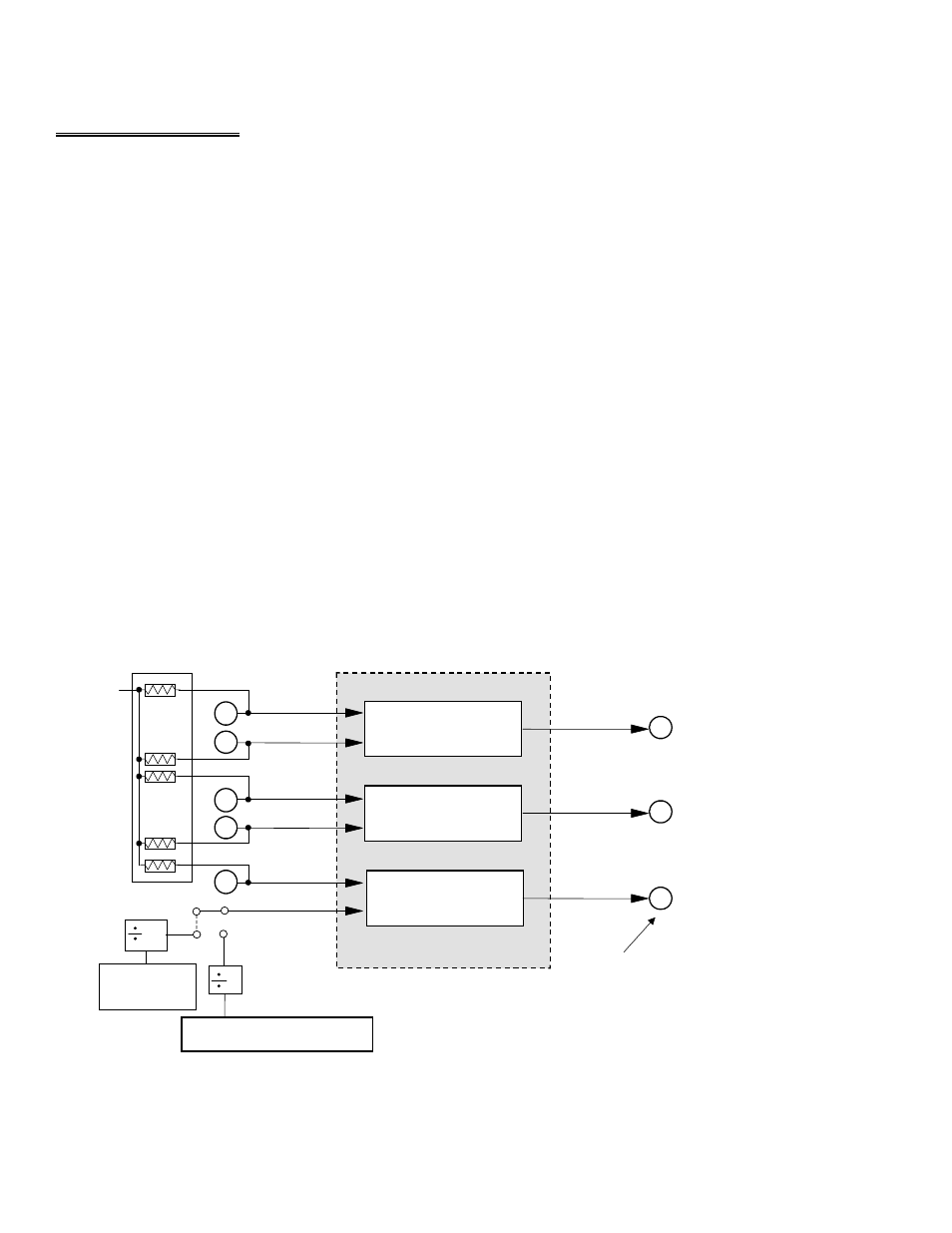
4.7 COUNTER/TIMER
The 82C54 counter/timer chip (Figure 4-1) may be used for event counting, frequency and pulse measurement and as a pacer
clock for the A/D converter. All the inputs, outputs and gates of the counter are accessible through the 37 pin analog connector
with the exception of the counter 2 input.
The counter is easy to understand. The GATE line determines whether or not TTL level pulses present at the CLK input will
decrement the counter. The OUT line then transitions (pulses or shifts) depending on the codes in the control register and the
count value in the count register.
The counter gates, inputs and outputs are all simple TTL.
The primary purpose of the counter timer chip is to pace the A/D samples. The input of counter 2 is jumper selectable for a
crystal controlled source or the PC bus clock source.
The PCLK signal is divided by 2 prior to the input at counter 2, therefore, if the PCLK signal on your PC/AT were 8 MHz, the
signal at the input of counter 2 would be 4MHz. The 10 MHz crystal source is divided by 10.
Assuming a 4 MHz signal at counter 2, the rates out of counter 2 (pin 6) can vary between 2 MHz (4 MHz / 2) to 61 Hz (4 MHz /
65,535). For rates slower than 61 Hz, wire the output of counter 2 to the input of counter 1. Next, wire the output of counter 1 to
the interrupt input (pin 24). The slowest rate is then once every 17 minutes.
When using the crystal source, the minimum rate would be about 15 Hz using only one counter.
COUNTER 0
COUNTER 1
COUNTER 2
PC BUS PCLK - B20
2
3
5
6
23
4
22
2
21
10K
+5
37 PIN
CON
U14
3
U8
RN1
GATE 0
CLK 0
GATE 1
CLK 1
GATE 2
CLK 2
10
10 MHz
CRYSTAL
CLK BUS
1 MHz
Figure 4-1. Counter /Timer Block Diagram
18