Register architecture – Measurement Computing CIO-DAS08-PGH User Manual
Page 17
4: REGISTER ARCHITECTURE
4.1 CONTROL & DATA REGISTERS
The CIO-DAS08-PGx is controlled and monitored by writing to and reading from eight consecutive 8-bit I/O addresses. The first
address, or BASE ADDRESS, is determined by setting a bank of switches on the board.
Register manipulation is best left to experienced programmerss as most of the possible functions are implemented in easy to use
Universal Library™.
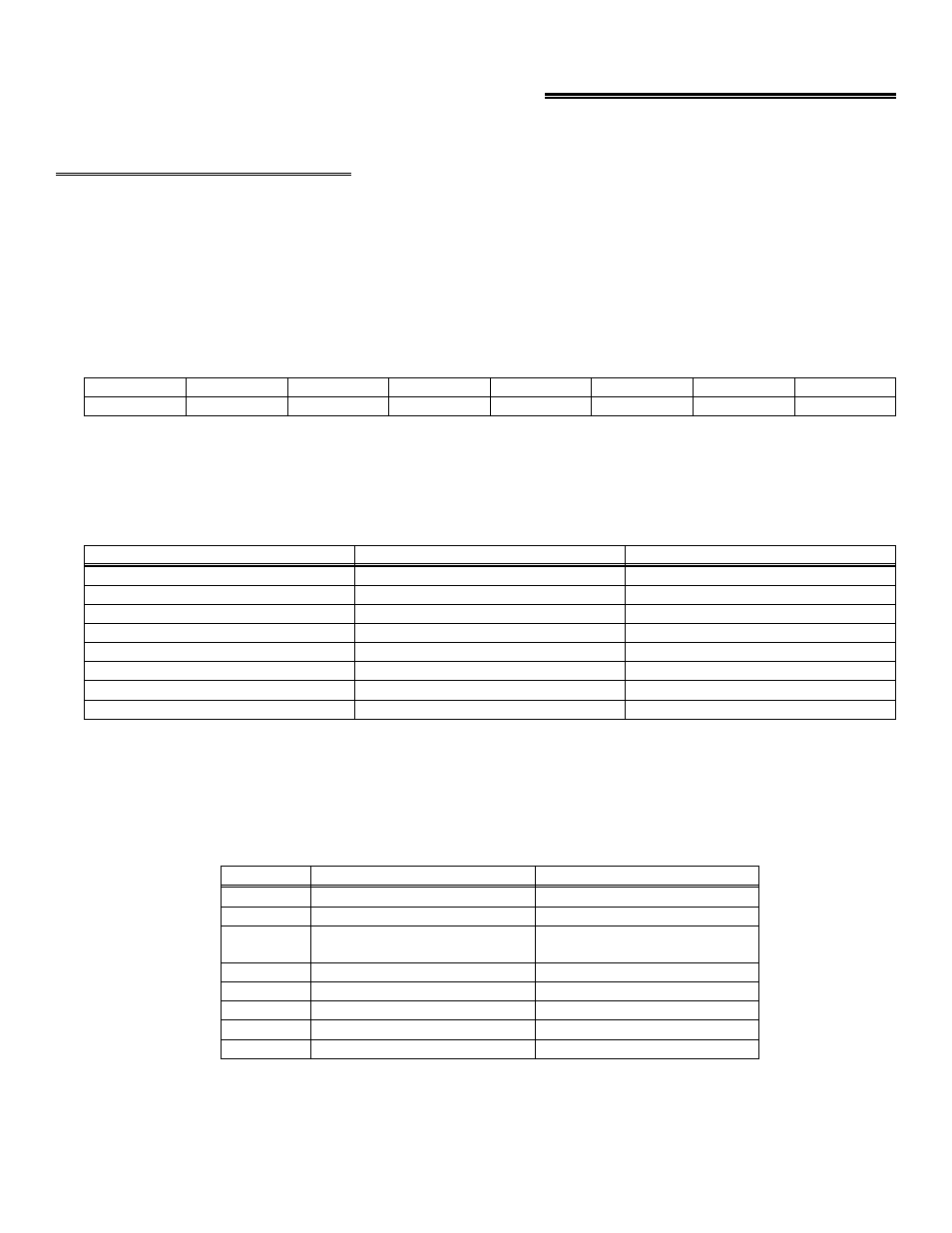
The register descriptions follow the format:
A/D8
A/D7
A/D6
A/D5
A/D4
A/D3
A/D2
A/D1
0
1
2
3
4
5
6
7
Where the numbers along the top row are the bit positions within the 8-bit byte and the numbers and symbols in the bottom row is
the function associated with each bit.
To write to or read from a register in decimal or HEX, the bit weights listed in table 4-1 apply.
Table 4-1. Register Bit Weights
80
128
7
40
64
6
20
32
5
10
16
4
8
8
3
4
4
2
2
2
1
1
1
0
HEX VALUE
DECIMAL VALUE
BIT POSITION
To write control words or data to a register, the individual bits must be set to 0 or 1 then combined to form a byte.
The method of programming required to read/write bits from bytes is beyond the scope of this manual.
In summary form, the registers and their function are listed in Table 4-2. Each register has eight bits which may constitute a byte
of data or eight individual bit read/write functions.
Table 4-2. Board Register Functions
Counter Control
Not Used
BASE +7
Load Counter 2
Read Counter 2
BASE +6
Load Counter 1
Read Counter 1
BASE +5
Load Counter 0
Read Counter 0
BASE +4
Programmable Gain Control
Channel MUX and Gain Status
BASE +3
OP1-OP4, INTE & MUX
Address
EOC, IP1-IP3, IRQ, MUX
Address
BASE +2
Start 12 Bit A/D Conversion
A/D Bits 1(MSB)-8
BASE +1
Start 8 Bit A/D Conversion
A/D Bits 9-12 (LSB)
BASE
WRITE FUNCTION
READ FUNCTION
ADDRESS
13