Measurement Computing CIO-DAS08-PGH User Manual
Page 18
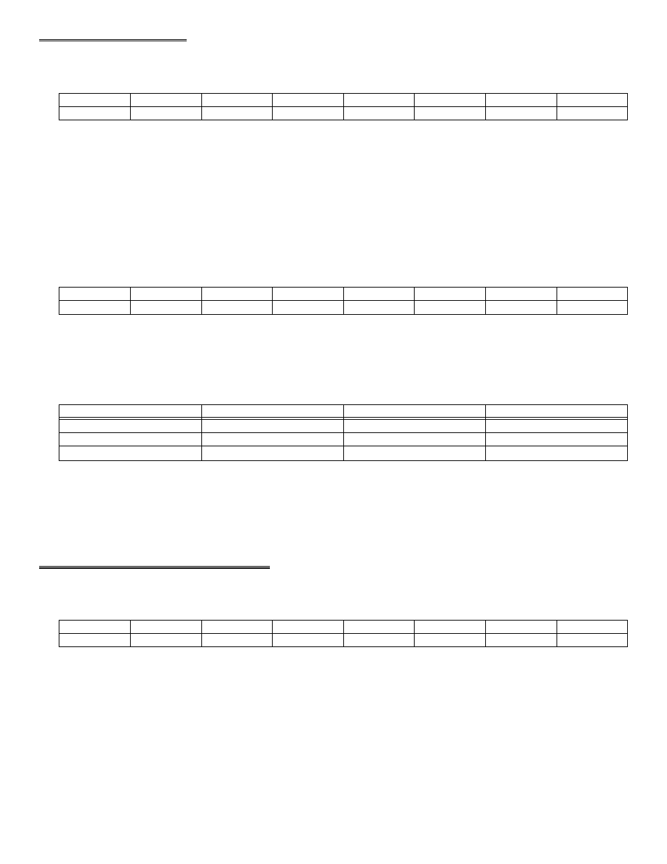
4.2 A/D DATA REGISTER
BASE ADDRESS (Read / Write)
0
0
0
0
A/D12 LSB
A/D11
A/D10
A/D9
0
1
2
3
4
5
6
7
READ
On read, it contains the least significant four digits of the analog input data.
These four bits of analog input data must be combined with the eight bits of analog input data in BASE + 1, forming a complete
12 bit number. The data is in the format 0 = minus full scale. 4095 = +FS.
WRITE
Writing any data to the register causes an immediate 8-bit A/D conversion.
BASE + 1 (Read / Write)
A/D8
A/D7
A/D6
A/D5
A/D4
A/D3
A/D2
A/D1 MSB
0
1
2
3
4
5
6
7
READ
On read, the most significant A/D byte is read.
The A/D Bits code corresponds to the voltage on the input according to the table below.
0 Volts
−
Full Scale
0
0
½ Full Scale
0 Volts
800
2048
+Full Scale
+Full Scale
FFF
4095
UNIPOLAR
BIPOLAR
HEX
DECIMAL
WRITE
Writing to this register starts a 12-bit A/D conversion.
A note of caution: Place several NO-OP instructions between consecutive 12-bit A/D conversions to avoid over-running the A/D
converter.
4.3 STATUS AND CONTROL REGISTER
BASE + 2 (Read / Write) Read Functions
MUX0
MUX1
MUX2
IRQ
IP1
IP2
IP3
EOC
0
1
2
3
4
5
6
7
READ = STATUS
EOC = 1 the A/D is busy converting and data should not be read.
EOC = 0 the A/D is not busy and data can be read.
IP3 to IP1 are the digital input lines on the 37 pin analog connector.
IRQ is the status of an edge triggered latch connected to Interrupt Input (pin 24) of the analog connector. It is high (1) when a
positive edge has been detected. It can be reset to 0 by writing to the INTE mask at BASE + 2 write.
14