Measurement Computing CIO-DAS08-AOH User Manual
Page 19
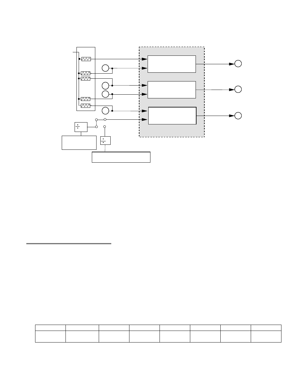
The primary purpose of the counter timer chip is to pace the A/D samples. The input of counter 2 is jumper selectable for a
crystal controlled source or the PC bus clock source.
Figure 6-1. 82C54 Counter/Timer Control
The PCLK signal is divided by two prior to the input at counter 2. Therefore, if the PCLK signal on your PC/AT were 8 MHz,
the signal at the input of counter 2 would be 4 MHz. The 10 MHz crystal source is divided by 10.
Assuming a 4 MHz signal at counter 2, the rates out of counter 2 (pin 6) may vary between 2 MHz (4 MHz / 2) to 61 Hz
(4 MHz / 65,535). For rates slower than 61 Hz, the output of counter 2 should be wired to the input of counter 1. The output
of counter 1 would then be wired to the interrupt input (pin 24). The slowest rate would then be once every 17 minutes.
When using the crystal source, the minimum rate would be about 15 Hz using only one counter.
6.8 D/A 0 CONTROL REGISTERS
Each D/A is controlled by a pair of 8-bit registers. These registers contain the low byte and the high nibble of the D/A 12-bit
control word. The value written to these two registers controls the output of the D/A chip relative to the range selected by the
D/A range select switch.
The D/A output range can generally be calculated as (#/4096) * FSR.
The #/4096 is a proportion of the Full Scale Range selected by the range switch.
Bipolar ranges are 0V at DAC value 2048.
BASE ADDRESS + 8, DAC 0 LOW BYTE (Read / Write)
DA0
LSb
DA1
DA2
DA3
DA4
DA5
DA6
DA7
0
1
2
3
4
5
6
7
15
COUNTER 0
COUNTER 1
COUNTER 2
PC BUS PCLK - B20
2
3
5
6
23
4
22
2
10K
+5
37 PIN
ANALOG
CONN. P2
U14
3
U8
RN1
GATE 0
CLK 0
GATE 1
CLK 1
GATE 2
CLK 2
10
0
10
MHz
OSCILLATOR
CLK BUS
1 MHz