Measurement Computing CIO-DAS08-AOH User Manual
Page 18
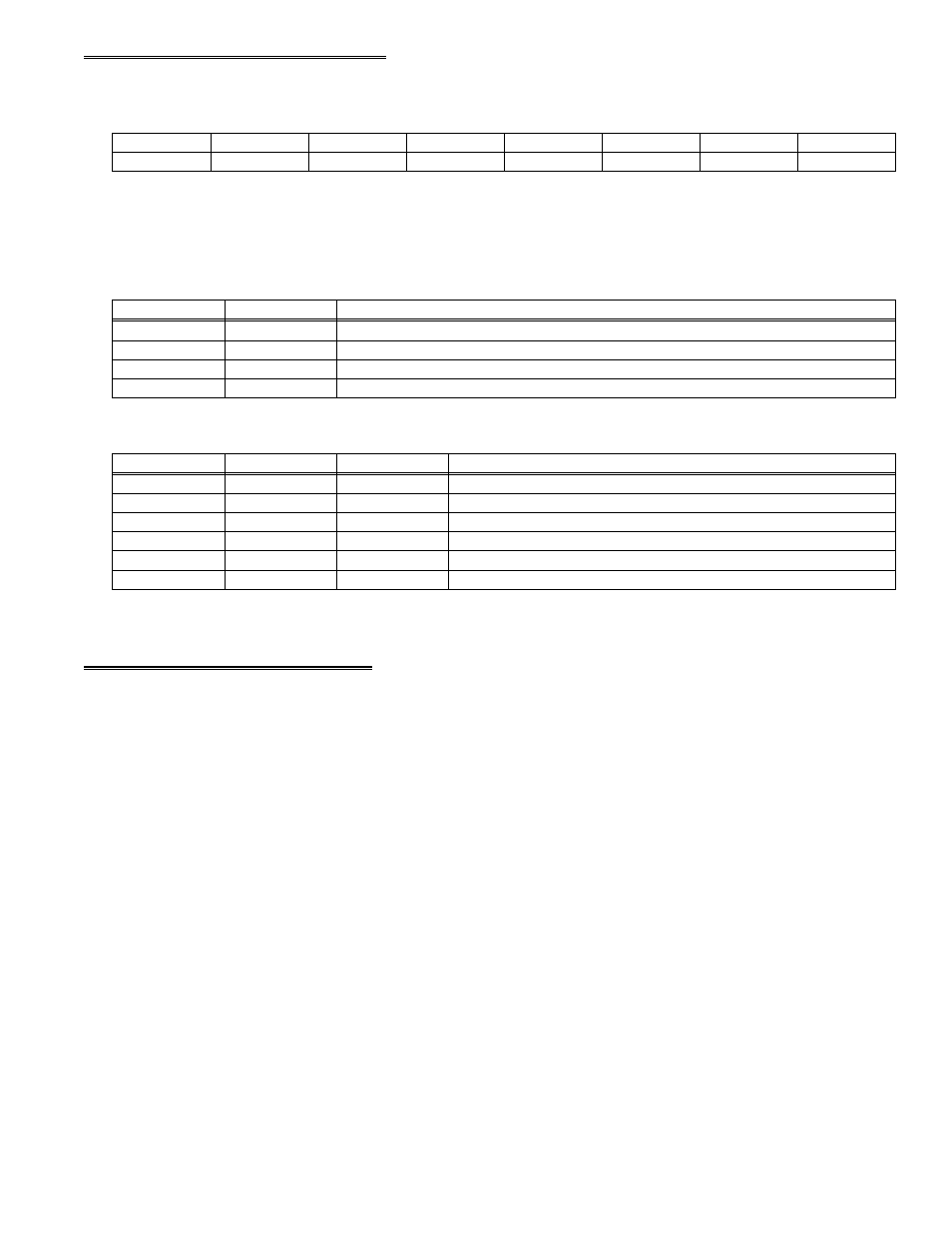
6.6 COUNTER CONTROL REGISTER
BASE ADDRESS + 7 (Write Only)
BCD
M0
M1
M2
RL0
RL1
SC0
SC1
0
1
2
3
4
5
6
7
WRITE
SC1 to SC0 are the counter select bits. They are binary-coded between 0 and 2.
RL1 to RL0 are the read and load control bits:
Read/load low the high byte (Word Transfer)
1
1
Read/load low byte
0
1
Read/load high byte
1
0
Latch counter
0
0
OPERATION
RL0
RL1
M2 to M0 are the counter control operation type bits:
Hardware triggered strobe
1
0
1
Software tirggered strobe
0
0
1
Square wave genrator
1
1
0
Rate generator
0
1
0
Programmable one-shot
1
0
0
Change on terminal count
0
0
0
OPERATION TYPE
M0
M1
M2
BCD = 0 then counter data is 16 bit binary. (65,535 max)
BCD = 1 then counter data is 4 decade Binary Coded Decimal. (9,999 max)
6.7 COUNTER TIMER OPERATION
The 8254 counter timer chip (Figure 6-1) can be used for event counting, frequency and pulse measurement and as a pacer
clock for the A/D converter. All the inputs, outputs, and gates of the counter are accessible through the 37-pin analog
connector with the exception of the counter 2 input.
The counter is easy to understand. The GATE line determines whether or not TTL level pulses present at the CLK input will
decrement the counter. The OUT line then transitions (pulses or shifts) depending on the codes in the control register and the
count value in the count register.
The counter gates, inputs and outputs are all simple TTL.
14