Test designs, Configuring the fpga using quartus ii programmer – Altera Transceiver Signal Integrity User Manual
Page 19
December 2011
Altera Corporation
Transceiver Signal Integrity Development Kit,
Stratix IV GX Edition User Guide
6. Stratix IV GX Transceiver Signal
Integrity Demonstration
The kit installs a demonstration application and test designs. The application
provides an easy-to-use interface where you can select various transceiver settings
and observe the result. Before you run the application and test designs, connect the
USB cable to the board and navigate to the Stratix IV GX Transceiver Signal Integrity
Demonstration application as explained in
“Installing the Transceiver Signal Integrity
Development Kit, Stratix IV GX Edition” on page 3–1
Test Designs
Altera provides a set of test designs for the evaluation of the Stratix IV GX device
transceiver performance and board features. The .sof file names and data rates for
each test design are listed in
. Before you run the application, use the
Quartus II Programmer to configure the Stratix IV GX device with one of the .sof files.
Configuring the FPGA Using Quartus II Programmer
It is sometimes necessary to use the Quartus II Programmer to configure the FPGA
with specific .sof files, such as the designs in
. Before configuring the FPGA,
ensure that the Quartus II Programmer and the USB-Blaster driver are installed on the
host computer and the development board is powered up.
To configure the Stratix IV GX FPGA, perform the following steps:
1. Start the Quartus II Programmer.
2. Click Add File and select the path to the desired .sof.
3. Turn on the Program/Configure option for the added file.
4. Click Start to download the selected file to the FPGA. The FPGA is configured
when the progress bar reaches 100%.
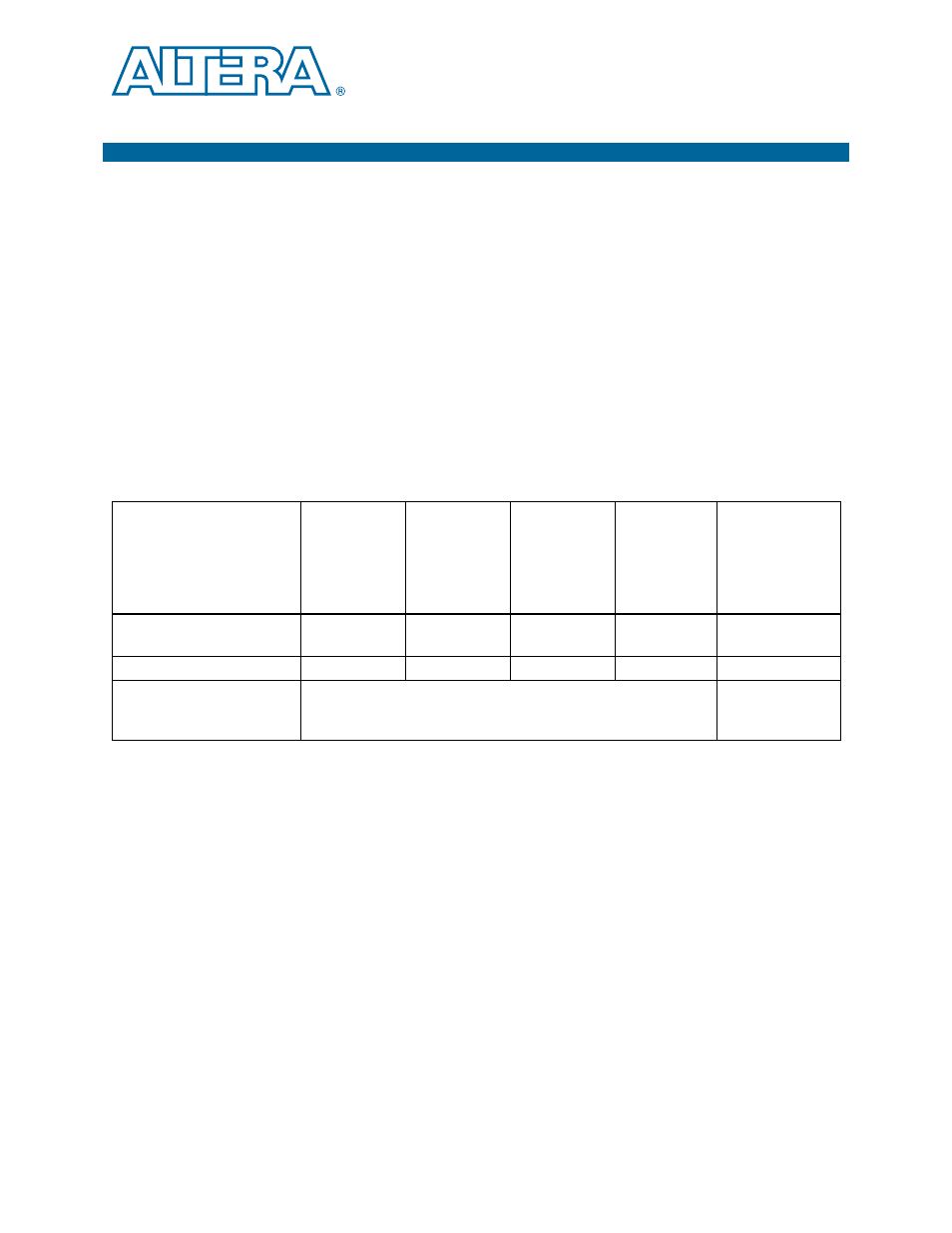
Table 6–1. Data Rates for Test Designs
File Name
Transceiver
Block 0
Channel 0
Data Rate
(Gbps)
Transceiver
Block 1
Channel 1,
Channel 2
Data Rate
(Gbps)
Transceiver
Block 1
Channel 3,
Channel 4
Data Rate
(Gbps)
Transceiver
Block 2
Channel 7
Data Rate
(Gbps)
Clocking scheme
signal_integrity_demo1.sof
soc_clk*20
3.125
PCI Express
(Gen1 or Gen2)
soc_clk*20
socket clock
signal_integrity_demo2.sof
soc_clk*20
soc_clk*20
soc_clk*20
soc_clk*20
socket clock
signal_integrity_demo3.sof
“Channel Reconfig Tab” on page 6–7
for the available
transceiver channel data rates and functional modes.
socket clock or
external SMA clock
(J19 and J20)
Note to
(1) The clock input is expected from the socketed oscillator (Y3) (soc_clk) on the board. If you are targeting –2 speed grade device on the board,
you can use 425 MHz. For –3 speed grade, the maximum data rate limit supported is 6.5 Gbps. Therefore, you must use 312.5 MHz (312.5*20
< 6.5 Gbps) and not the 425-MHz clock crystal.