Flash programmer target design, Flash programmer target design –3, Figure 1–1 – Altera Nios II User Manual
Page 7
Chapter 1: Overview of the Nios II Flash Programmer
1–3
How the Flash Programmer Works
© March 2014
Altera Corporation
Nios II Flash Programmer User Guide
Flash Programmer Target Design
To use the Nios II Flash Programmer, you must have a valid flash programmer target
design downloaded to your board. A valid target design contains a Qsys system with
at least the Qsys components shown in
The minimum component set provides facilities for the target design to communicate
with the host and to write to flash memory. The minimum component set depends on
the type of flash memory you intend to program.
lists the minimum
component set for programming each kind of flash memory.
shows an example of a Qsys system containing the minimum component
set for a system with one CFI flash memory and an EPCS serial configuration device.
The system also includes other components which relate to the purpose of the system,
not to the flash programmer.
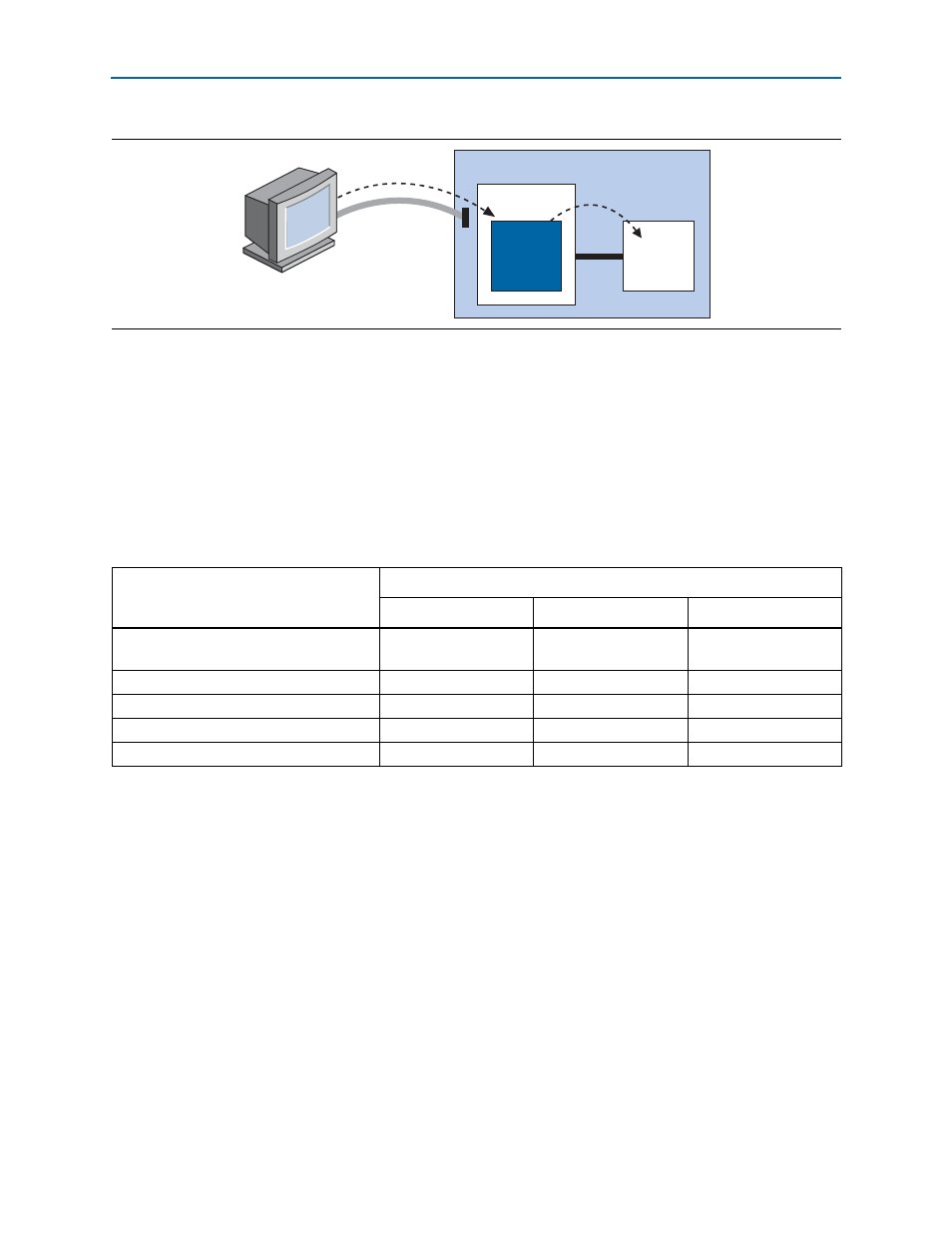
Figure 1–1. How the Nios II Flash Programmer Works
Target Board
Flash
Memory
Device
Download Cable
(e.g. USB Blaster)
Altera FPGA
Target
Design
Flash
Content
Host Computer
Flash
Content
Table 1–1. Minimum Component Set for the Flash Programmer Target Design
Component
Flash Memory to Program
CFI Only
EPCS Only
CFI and EPCS
Nios II processor, with JTAG debug module
level 1 or greater
Required
Required
Required
System ID peripheral
Recommended
Recommended
Recommended
Flash Memory (Common Flash Interface)
Required
Required
Tristate Conduit Bridge
Required
Required
EPCS Serial Flash Controller
Required
Required
Notes to
:
(1) If present, a System ID Peripheral component allows the Nios II Flash Programmer to validate the target design before programming the flash
memory.
(2) A Nios II system can interface with more than one CFI flash memory device. The system must contain one Flash Memory (Common Flash
Interface) component for each flash memory device on the board.
(3) Tri-state Conduit Bridge is needed to drive the CFI flash memory signals.