Tutorial: mixing sstl and lvttl in a single bank – Altera Early SSN Estimator User Manual
Page 11
© November 2009
Altera Corporation
Early SSN Estimator User Guide for Altera Programmable Devices
2. Tutorial: Mixing SSTL and LVTTL in a
Single Bank
This tutorial describes how you can add ten 1.8-V LVTTL pins to a bank filled with ten
1.8-V SSTL Class I 12 mA and ten 1.8-V SSTL Class II 16 mA drivers. In this tutorial
you are targeting a voltage margin of 225 mV to account for other non-SSN related
items. Use the ESE to determine if you might have problems.
Step 1: Configure the Global Parameters
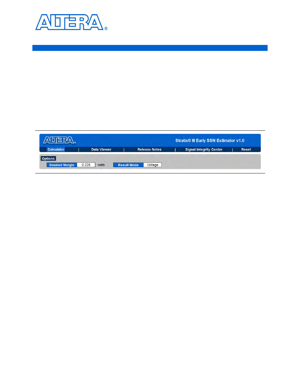
1. Configure result mode to display the results in Voltage.
2. Enter a desired margin of 0.225 volts, as shown in
Step 2: Assign I/O Standards to the Corresponding Bank
1. Set the I/O Bank 1a VCCIO to 1.8 V.
2. Select the I/O Standard SSTL Class I in row one.
3. Select a drive strength of 12 mA.
4. Select Fast slew rate.
1
Not all Altera device families have the slew rate control option.
5. Enter 10 as the number of output pins.
6. Select the I/O Standard SSTL Class II in row two.
7. Select a drive strength of 16 mA.
8. Select Fast slew rate.
1
Not all Altera device families have the slew rate control option.
9. Enter 10 as the number of output pins.
10. Select the I/O standard LVTTL in row three.
11. Select a drive strength of 12 mA.
12. Select Fast slew rate.
1
Not all Altera device families have the slew rate control option.
13. Enter 10 as the number of output pins, as shown in
.
Figure 2–1. Global Parameters Configuration