Pdn circuit topology, Ztarget, Pdn circuit topology –2 – Altera Device-Specific Power Delivery Network User Manual
Page 6
1–2
Chapter 1: User Guide for the Device-Specific Power Delivery Network (PDN) Tool
PDN Decoupling Methodology Review
Device-Specific Power Delivery Network (PDN) Tool User Guide
September 2012
Altera Corporation
PDN Circuit Topology
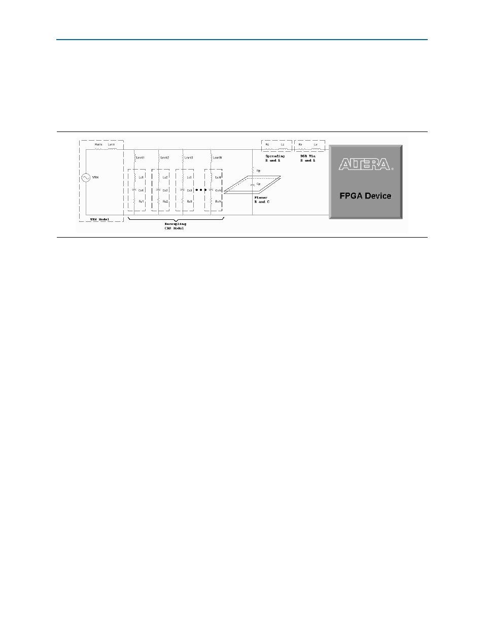
The PDN tool is based on a lumped equivalent model representation of the power
delivery network topology.
shows a schematic representation of the circuit
topology, modeled as part of the tool. The PDN impedance profile is the
impedance-over-frequency looking from the device side.
For first order analysis, the voltage regulator module (VRM) can be simply modeled
as a series connected resistor and inductor, as shown in
. At low
frequencies, up to approximately 50 KHz, the VRM has a very low impedance and is
capable of responding to the instantaneous current requirements of the FPGA. The
equivalent series resistance (ESR) and equivalent series inductance (ESL) values can
be obtained from the VRM manufacturer. At higher frequency, the VRM impedance is
primarily inductive, making it incapable of meeting the transient current requirement.
PCB decoupling capacitors are used for reducing the PDN impedance up to tens of
MHz. The on-board discrete decoupling capacitors provides the required low
impedance depending on the capacitor intrinsic parasitics (R
cN
, C
cN
, L
cN
) and the
capacitor mounting inductance (L
mntN
). The inter-planar capacitance between the
power-ground planes typically has lower inductance than the discrete decoupling
capacitor network, making it more effective at higher frequencies (tens of MHz). As
frequency increases (tens of MHz and above), the PCB decoupling capacitors become
less effective. The limitation comes from the parasitic inductance seen with respect to
the FPGA, which consists of capacitor mounting inductance, PCB spreading
inductance, ball grid array (BGA) via inductance, and packaging parasitic inductance.
All these parasitics are modeled in this PDN tool to capture the effect of the PCB
decoupling capacitors accurately. To simplify the circuit topology, all parasitics are
represented with lumped inductors and resistors despite the distributed nature of
PCB spreading inductance.
Z
TARGET
According to Ohm’s law, voltage drop across a circuit is proportional to the current
flow through the circuit and impedance of the circuit. The transient component of
PDN current gives rise to voltage fluctuation within the PDN, which may lead to logic
and timing issues. You can reduce excessive voltage fluctuation by reducing PDN
impedance. One design guide line is target impedance Z
TARGET
.
Figure 1–1. PDN Topology