Device/power rail information, Component parameters setting – Altera Device-Specific Power Delivery Network User Manual
Page 18
1–14
Chapter 1: User Guide for the Device-Specific Power Delivery Network (PDN) Tool
Major Tabs of the PDN Tool
Device-Specific Power Delivery Network (PDN) Tool User Guide
September 2012
Altera Corporation
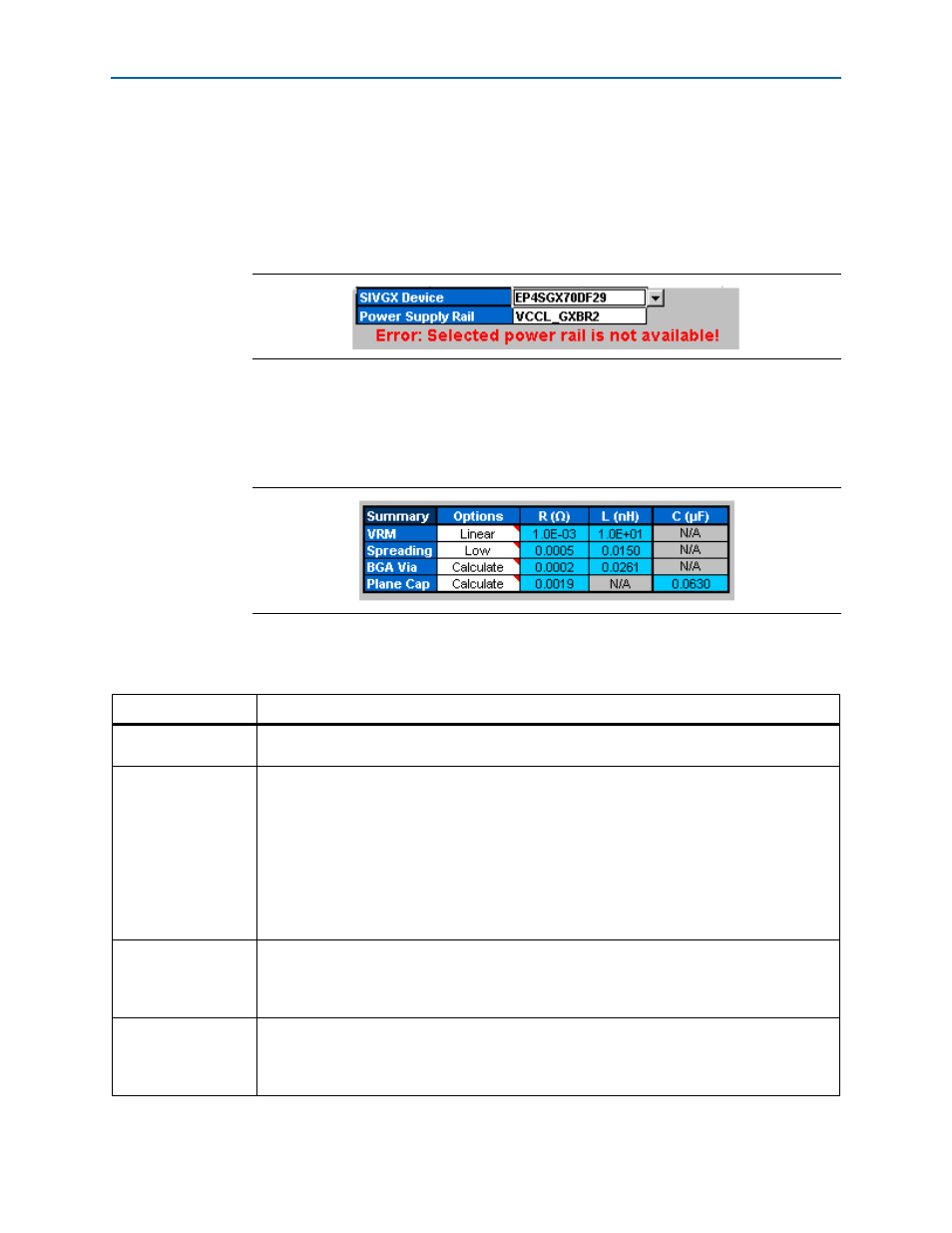
Device/Power Rail Information
You select the device/power rail to work in this field. A pull-down menu with the
names of the available devices and power rails in the Altera device family supported
by the tool is shown when you click the corresponding cell. The tool validates the
selected device/power rail combination. A warning is shown beneath the field if an
invalid combination is chosen (
).
Component Parameters Setting
You can either enable or disable the following components of the PDN network
shown in
describes the PDN components.
Figure 1–9. Device/Power Rail Information
Figure 1–10. Parameter Settings for PDN Components
Table 1–3. Parameters of PDN Components
Parameter Description
VRM
to disable this component, select Ignore. To enable the VRM parasitics, select Linear, Switcher, or
Custom.
Spreading
Based on the design, you can select either Low, Medium, High, or a Custom value for the effective
spreading R, L values that the decoupling capacitors see with respect to the FPGA. You can also
ignore the spreading inductance by selecting Ignore. Ignoring the spreading inductance leads to
an optimistic result and is not an accurate representation of the impedance profile that the FPGA
sees.
The Ignore option helps you understand that the spreading inductance in combination with the
BGA via inductance is the limiting factor from a PCB perspective to decouple the FPGA at high
frequencies. Be careful when choosing the Ignore option while coming up with a final capacitor
count.
BGA Via
Based on the design, you can choose to Ignore the BGA via component or to Calculate the
effective via inductance based on the layout. If you are in the middle of layout, you can directly
enter the effective loop R, L via parasitics in the Library tab and choose the Custom setting under
BGA Via to include the via parasitics.
Plane Capacitance
Based on the design, you can either choose to Ignore the inter-planar capacitance between the
power and ground plane, or Calculate the plane capacitance based on the layout. If you are in the
middle of layout, you can directly enter the plane capacitance in the Library tab and choose the
Custom setting under the Plane Cap to include the plane capacitance parasitics.