The clock control, The clock control –12 – Altera Cyclone V E FPGA User Manual
Page 28
6–12
Chapter 6: Board Test System
The Clock Control
Cyclone V E FPGA Development Kit
December 2014
Altera Corporation
User Guide
The Clock Control
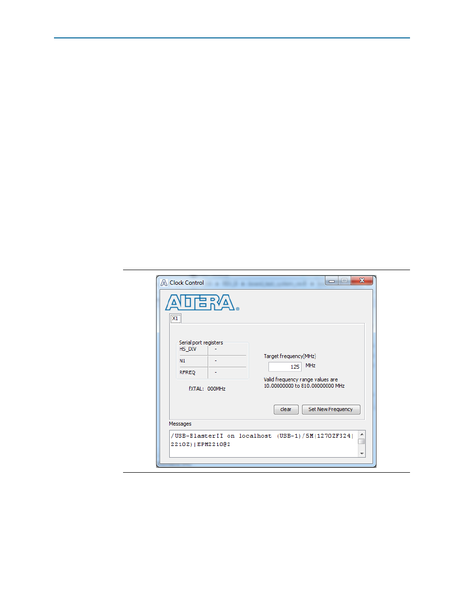
The Clock Control application sets the Si570 programmable oscillator to any
frequency between 10 MHz and 810 MHz with eight digits of precision to the right of
the decimal point. The default frequency for the oscillator is 125 MHz.
The Si570 device has one programmable output. The output of the Si570 drives a
1-to-4 clock fanout buffer that drives the top and bottom banks of the FPGA.
The Clock Control application runs as a stand-alone application. ClockControl.exe
resides in the
Windows, click Start > All Programs > Altera > Cyclone V E FPGA Development
Kit
<version> > Clock Control to start the application.
f
For more information about the
Si570
and the Cyclone V E FPGA development
board’s clocking circuitry and clock input pins, refer to the
.
The Clock Control communicates with the
MAX V device on the board through the
JTAG bus. The Si570 programmable oscillator is connected to the MAX V device
through a 2-wire serial bus.
The following sections describe the Clock Control controls.
Figure 6–6. The Clock Control