Functional description, Building blocks of a pll, A pre-scale counter – Altera I/O Phase-Locked Loop (Altera IOPLL) IP Core User Manual
Page 7: And post-scale counters
Altera IOPLL IP Core Parameters - Advanced Parameters Tab
Table 5: Altera IOPLL IP Core Parameters - Advanced Parameters Tab
Parameter
Legal Value
Description
Advanced Parameters
—
Displays a table of physical PLL settings that will be
implemented based on your input.
Functional Description
An I/O PLL is a frequency-control system that generates an output clock by synchronizing itself to an
input clock. The PLL compares the phase difference between the input signal and the output signal of a
voltage-controlled oscillator (VCO) and then performs phase synchronization to maintain a constant
phase angle (lock) on the frequency of the input or reference signal. The synchronization or negative
feedback loop of the system forces the PLL to be phase-locked.
You can configure PLLs as frequency multipliers, dividers, demodulators, tracking generators, or clock
recovery circuits. You can use PLLs to generate stable frequencies, recover signals from a noisy communi‐
cation channel, or distribute clock signals throughout your design.
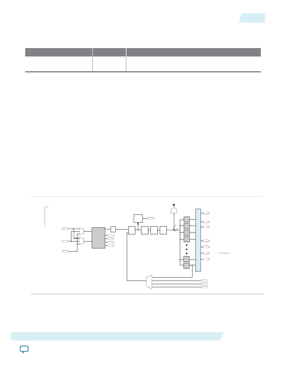
Building Blocks of a PLL
The main blocks of the I/O PLL are the phase frequency detector (PFD), charge pump, loop filter, VCO,
and counters, such as a feedback counter (
M
), a pre-scale counter (
N
), and post-scale counters (
C
). The PLL
architecture depends on the device you use in your design.
Figure 1: Typical I/O PLL Architecture
Clock
Switchover
Block
inclk0
inclk1
Cascade Input
from Adjacent I/O PLL
and Dedicated refclk
clkswitch
clkbad0
clkbad1
activeclock
PFD
Lock
Circuit
locked
÷N
CP
LF
VCO
GCLK/RCLK
4
FBIN
LVDS Clock Network
GCLK/RCLK Network
Direct Compensation Mode
Zero Delay Buffer, External Feedback Modes
LVDS Compensation Mode
Source Synchronous, Normal Modes
÷C0
÷C1
÷C2
÷C3
÷C8
÷M
PLL O
utput Multiple
xer
Casade Output
to Adjacent I/O PLL
GCLKs
RCLKs
FBOUT
External Memory
Interface DLL
8
8
To DPA Block
RX/TX Clock
RX/TX Load Enable
For single-ended clock inputs, only the CLKp pin
has a dedicated connection to the PLL. If you use the
CLKn pin, a global or regional clock is used.
Dedicated Clock Inputs
This FBOUT port is fed by
the M counter in the PLLs.
UG-01155
2015.05.04
Altera IOPLL IP Core Parameters - Advanced Parameters Tab
7
Altera I/O Phase-Locked Loop (Altera IOPLL) IP Core User Guide
Altera Corporation