Opgp-34-a4b3ra, Pin description – Delta Electronics GPON ONU Transceiver OPGP-34-A4B3RA User Manual
Page 5
OPGP-34-A4B3RA
DELTA ELECTRONICS, INC.
5 Revision:
S2
12/26/2006
www.deltaww.com
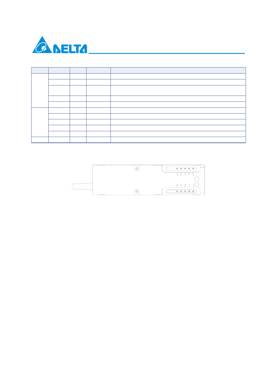
7. Pin Description
Tx/Rx Pin No.
I/O Pin Name
Description
1
VeeR
Receiver Ground
2
VccR
+3.3V Receiver Power Supply
3 O
SD
Normal Optical Input indicated by logic “High”, and No Optical
Input indicated by logic “Low”. (LVTTL)
4 O
RD(n)
Inverted Receiver Data Output (AC-Coupled CML output)
Rx
5 O
RD(p)
Non-Inverted Receiver Data Output (AC-Coupled CML output)
6
VccT
+3.3V Transmitter Power Supply
7
VeeT
Transmitter Ground
8 I
BiasCNT
Positive pulse which control the ONU burst mode operation
9 I
TD(p)
Non-Inverted Transmitter Data Input (DC-Coupled LVPECL input)
Tx
10 I
TD(n)
Inverted Transmitter Data Input (DC-Coupled LVPECL input)
MS
Mounting studs/ connect this pin to Chassis ground
Bottom View
MS
MS
- 1x9 Bi-Directional Transceiver Module OPBD-155F2J1R (7 pages)
- Single Mode SFP Transceiver LCP-1250B4MDRx (14 pages)
- LC-1250xxxx Series (10 pages)
- Human Machine Interface DOP-AS Series (329 pages)
- Analog Output Module DVP04DA-S (2 pages)
- DeviceNet Slave Communication Module IFD9502 (2 pages)
- LCP-155B4MSRx (12 pages)
- High-Speed PCI 12-Axis Motion Control Card PCI-DMC-B01 (528 pages)
- Network Device DVP01PU-S (2 pages)
- GBIC-1250D5MR (12 pages)
- SPBD-1250A4Q1RT (10 pages)
- SILM4015 (1 page)
- LCP-8500A4EDR (14 pages)
- 10GBASE-SR SFP+ Optical Transceiver LCP-10G3A4EDR (16 pages)
- LCP-155A4HSRx (11 pages)
- LCP-1250RJ3SR-L (9 pages)
- SILM320L (1 page)
- LCP-1250RJ3SR-S (9 pages)
- SIL530 (1 page)
- Extension Digital I/O Module DOP-EXIO28RAE (1 page)
- DVP Series PLC DVP04TC-H2 (2 pages)
- 1x9 Bi-Directional Transceiver Module OPBD-155F1J1R (7 pages)
- Distribution Box TAP-CN01/02/03 (2 pages)
- LCP-200A4HSR (9 pages)
- Pulse Generation Unit DVP01PU-H2 (2 pages)
- Power Connection Interface VFD-PSD01 (1 page)
- Programmable Logic Controller DVP04DA-H2 (2 pages)
- Single Mode SFP Transceiver LCP-1250B4QDRx (13 pages)
- LCP-155B4JSRx Series (12 pages)
- Series Temperature Controller DTD Series (2 pages)
- Brake Modules BUE Series (2 pages)
- PLC DVP Series DVP-SX (2 pages)
- Digital Keypad / Display ASD-PU-01A (1 page)
- Multimode SFP Transceiver LCP-1250A4FDRx (14 pages)
- HMU1362M (1 page)
- RPA-01 (1 page)
- THMR1395 (1 page)
- SFBD-155F2J1RM (7 pages)
- Program Transfer Module DVP-PCC01 (1 page)
- RTU-DNET (41 pages)
- AC Servo Drive ASDA-AB (37 pages)
- Digital Keypad / Display ASD-PU-01B (1 page)
- HMR1045 (1 page)
- CANopen Communication Module DVPCOPM-SL (2 pages)
- SPBD-1250B4Q1R (10 pages)