ADLINK ETX-BT User Manual
Page 17
Page 17
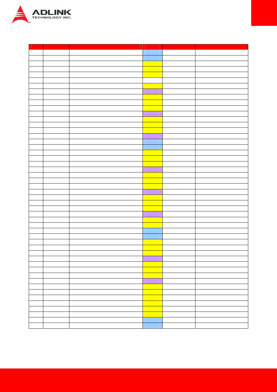
Pin
Signal
Description
Type
PU/PD
Comment
51 5VCC Power
+5V
PWR
52 5VCC Power
+5V
PWR
53
PAR
PCI Bus Parity
IO-3,3
54
SERR#
PCI Bus System Error
IO-3,3
PU 8k2 3,3V
55
GPERR#
PCI Bus Grant Error
IO-3,3
PU 8k2 3,3V
56 RESERVED
NC
-
57
PME#
PCI Power Management Event
IO-3,3
PU 10k 3,3VSB
-
58
USB2N
USB Data- Port2
I/O - DP
59
LOCK#
PCI Bus Lock
IO-3,3
PU 8k2 3,3V
60
DEVSEL#
PCI Bus Device Select
IO-3,3
PU 8k2 3,3V
61
TRDY#
PIC Bus Target Ready
IO-3,3
PU 8k2 3,3V
62
USB3N
USB Data- Port3
I/O - DP
63
IRDY#
PCI Bus Initiator Ready
IO-3,3
PU 8k2 3,3V
64
STOP#
PCI Bus Stop
IO-3,3
PU 8k2 3,3V
65
FRAME#
PCI Bus Cycle Frame
IO-3,3
PU 8k2 3,3V
66
USB2P
USB Data+ Port2
I/O - DP
67 GND Ground
PWR
68 GND Ground
PWR
69
AD16
PCI Address & Data Bus line
IO-3,3
70
CBE2#
PCI Bus Command and Byte enables 2
IO-3,3
71
AD17
PCI Address & Data Bus line
IO-3,3
72
USB3P
USB Data+ Port3
I/O - DP
73
AD19
PCI Address & Data Bus line
IO-3,3
74
AD18
PCI Address & Data Bus line
IO-3,3
75
AD20
PCI Address & Data Bus line
IO-3,3
76
USB0N
USB Data- Port0
I/O - DP
77
AD22
PCI Address & Data Bus line
IO-3,3
78
AD21
PCI Address & Data Bus line
IO-3,3
79
AD23
PCI Address & Data Bus line
IO-3,3
80
USB1N
USB Data- Port1
I/O - DP
81
AD24
PCI Address & Data Bus line
IO-3,3
82
CBE3#
PCI Bus Command and Byte enables 3
IO-3,3
83 5VCC Power
+5V
PWR
84 5VCC Power
+5V
PWR
85
AD25
PCI Address & Data Bus line
IO-3,3
86
AD26
PCI Address & Data Bus line
IO-3,3
87
AD28
PCI Address & Data Bus line
IO-3,3
88
USB0P
USB Data+ Port0
I/O - DP
89
AD27
PCI Address & Data Bus line
IO-3,3
90
AD29
PCI Address & Data Bus line
IO-3,3
91
AD30
PCI Address & Data Bus line
IO-3,3
92
USB1P
USB Data+ Port1
I/O - DP
93
PCIRST#
PCI Bus Reset
O-3,3
94
AD31
PCI Address & Data Bus line
IO-3,3
95
INTC#
PCI BUS Interrupt Reauest C
I-3,3
PU 8k2 3,3V
96
INTD#
PCI BUS Interrupt Reauest D
I-3,3
PU 8k2 3,3V
97
INTA#
PCI BUS Interrupt Reauest A
I-3,3
PU 8k2 3,3V
98
INTB#
PCI BUS Interrupt Reauest B
I-3,3
PU 8k2 3,3V
99 GND Ground
PWR
100 GND Ground
PWR