ADLINK ASD8P-MT1 Series User Manual
Page 23

ASD8P-MT1 Specification
Page 23 of 43
Additionally, the device must ensure that it does not pull CLKREQ# low unless CLKREQ# is being
intentionally asserted in all cases; including when the related function is in D3cold. This means
that any component implementing CLKREQ# must be designed such that:
Unpowered CLKREQ# output circuits are not damaged if a voltage is applied to them
from other powered “wire-ORed” sources of CLKREQ#.
When power is removed from its CLKREQ# generation logic, the unpowered output
does not present a low impedance path to ground or any other voltage.
These additional requirements ensure that the CLKREQ# signal network continues to function
properly when a mixture of powered and unpowered components have their CLKREQ# outputs
wire-ORed together. It is important to note that most commonly available open drain and tri-state
buffer circuit designs used “as is” do not satisfy the additional circuit design requirements for
CLKREQ#.
Power-up Requirements
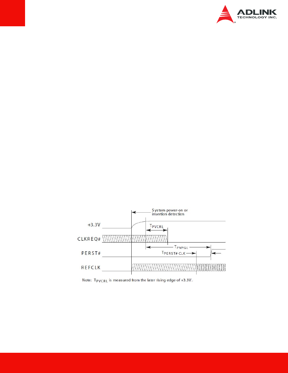
CLKREQ# is asserted in response to PERST# assertion. On power up, CLKREQ# must be
asserted by a PCI Express device within a delay (TPVCRL) from the power rails achieving
specified operating limits and PERST# assertion (see Figure 78). This delay is to allow adequate
time for the power to stabilize on the card and certain system functions to start prior to the card
starting up. CLKREQ# may not be de-asserted while PERST# is asserted.
Dynamic Clock Control
After a PCI Express device has powered up and whenever its upstream link enters the L1 link
state, it shall allow its reference clock to be turned off (put into the parked clock state). To
accomplish this, the device de-asserts CLKREQ# (high) and must allow that the reference clock
will transition to the parked clock state within a delay (TCRHoff). Figure 79 shows the CLKREQ#
clock control timing diagram.
