3 architecture, 4 power mode support – ADLINK ASD8P-MT1 Series User Manual
Page 17
ASD8P-MT1 Specification
Page 17 of 43
2.3 Architecture
The ASD8P-MT1 PCIe Gen2 x 2 Lane Solid State Drive (SSD) utilizes a cost effective system-on-
chip (SoC) design to provide a full 1GB/s bandwidth with the host while managing multiple flash
memory devices on multiple channels internally.
2.4 Power Mode Support
PCI Express feature enables the hardware to engage actively in automatic Link power
management.
ASD8P-MT1 PCIe Gen2 x 2 Lane SSD Supports L0, L0s and L1 mode.
z
L0: Full On (Active power / Active mode)
z
L0s: Idle (Lower power / Idle mode)
z
L1: Idle (Lower power / sleep mode)
The Link state transits automatically from L0 (full on) to an L0s/L1 (idle) state to save power when
there is no data transferring. T
he device reduces power by gating internal clocks, and the
CLKREQ# signal
transited by host
will enable lower power mode of some internal components
such as PCIe PHY.
Once the data can be transferred across the Link, the state will be brought
back to L0 by the hardware.
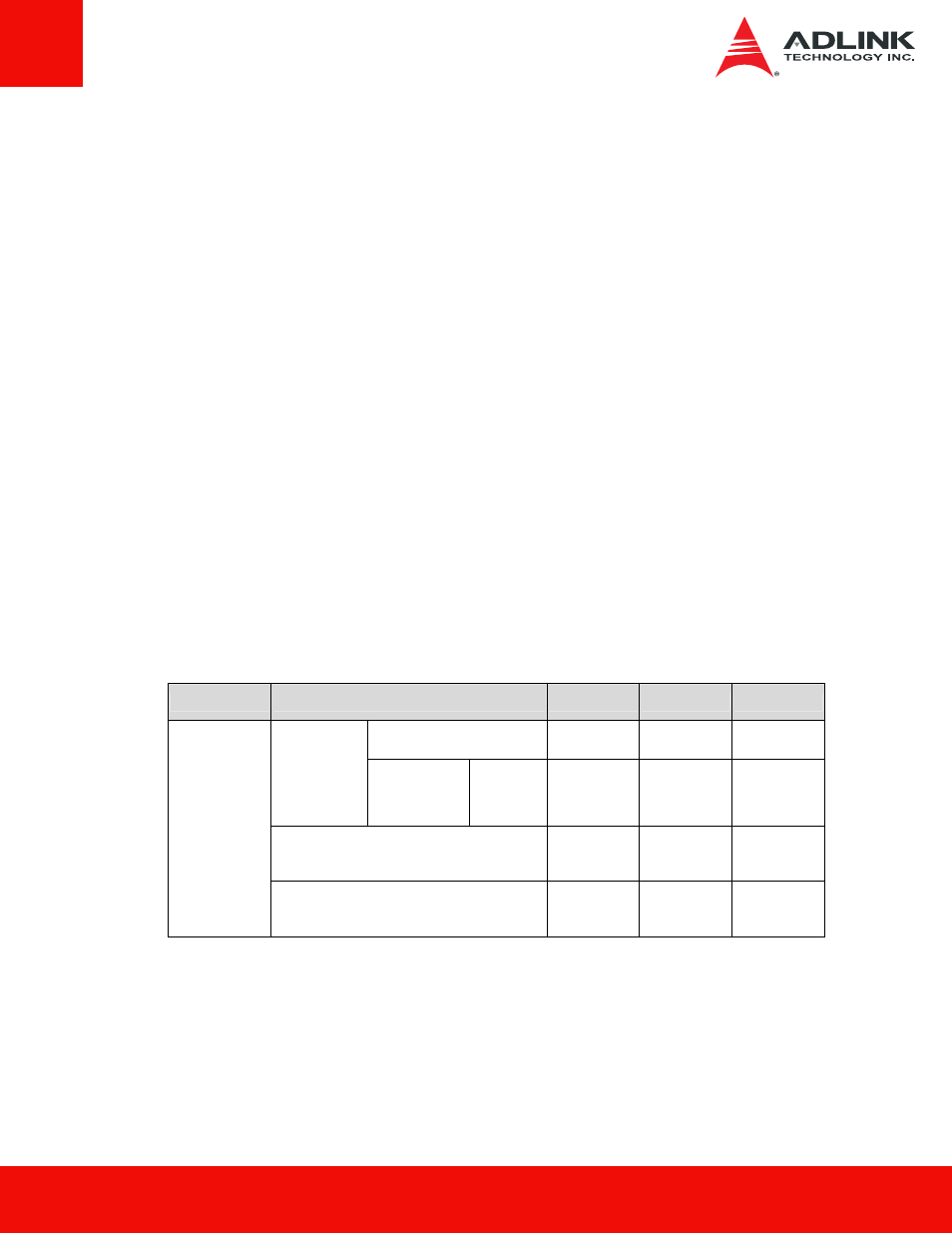
Input Voltage
State
128GB
256GB
512GB
After power-on
0. 66
0. 69
0. 73
Active Mode
(L0 state)
Max.
Read/Write
Performance
rms
3. 2
3. 2
3. 5
Idle Mode
(L0s state)
0. 58
0. 60
0. 60
3. 3V ± 5%
Sleep Mode
(L1 state)
0. 13
0. 13
0. 14
• Units: W
• L0 stands for power states after power-on and before entering L0s/L1,
• To enable L1 lower mode, the CLKREQ# signal must be sent by host.