2 layer stack-up, Outline, 1 board – ADLINK aTCA-N700 User Manual
Page 54
aTCA-RN720 User's Guide
54
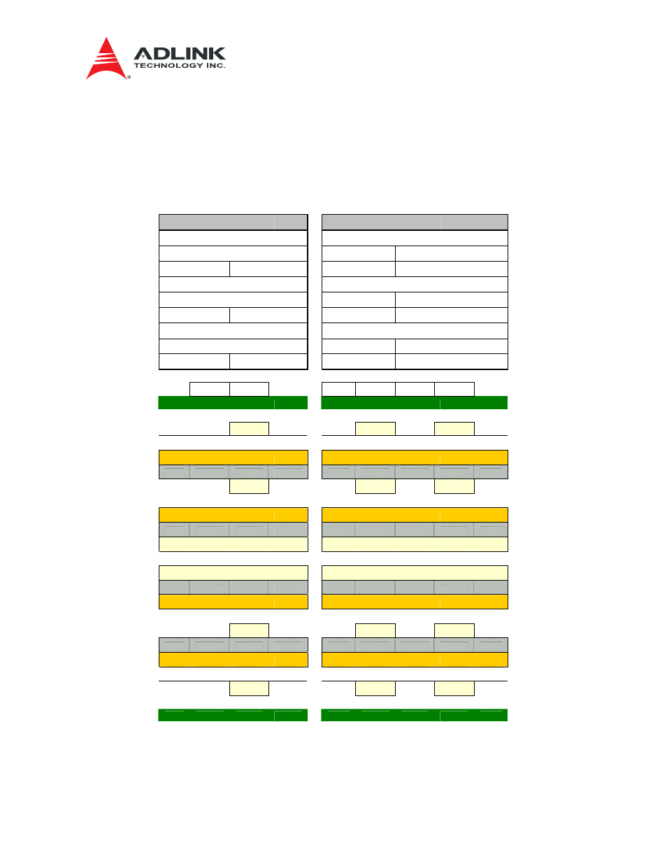
11.2 Layer Stack-up
The layering of the PCB is illustrated in Figure 11-2.The blade has 10layers of PCB laminate with
FR408HR material, which has a low dielectric constant and low dissipation factor that are
adequate to support 10Gbps SerDes signals.
Design Specifications
Design Specifications
Lyrs: 1L(Ref 2L) & 10L(Ref 9L)
Lyrs:
1L(Ref 2L) & 10L(Ref 9L)
Line: 5.30mil
Line:
3.70mil Space: 6.30mil
Zo: 50Ω Tol:
10%
Zd:
100Ω Tol: 10%
Lyrs: 3L(Ref 2L & 4L)
Lyrs:
3L(Ref 2L & 4L)
Line: 6.10mil
Line:
4.35mil Space: 5.65mil
Zo: 50Ω Tol:
10%
Zd:
100Ω Tol: 10%
Lyrs
8L(Ref 7L & 9L)
Lyrs
8L(Ref 7L & 9L)
Line
6.10mil
Line
4.35mil Space: 5.65mil
Zo: 50Ω Tol:
10%
Zd:
100Ω Tol: 10%
Zo Line
Zd Line Space Line
1
49.9
5.30
100.1
3.70 6.30
3.70
10.00
1
2
2
3
50.0
6.10
99.8
4.35 5.65
4.35
10.00
3
4
4
5
5
6
6
7
7
8
50.0
6.10
99.8
4.35 5.65
4.35
10.00
8
9
9
10
49.9
5.30
100.1
3.70 6.30
3.70
10.00
10
Figure 11-2 PCB Layer Stack-up