Power-up do setup/read back register – ADLINK PCI-7442 User Manual
Page 71
Register Format
59
Power-up DO Setup/Read Back Register
After the system powers up, the PCI-7444 can enter the initial pro-
cedure which sends out the default initial value to 128-CH digital
outputs. You can configure the default power-up DO values and
store them in the flash memory to prevent the DO from entering an
unknown status when the system turns on.
You may set the 128-CH power-up default DO values by access-
ing the Power-up DO Setup Registers in turn. After accessing the
latest Power-up DO Setup Register (Base+0x24h), the card
needs at least 500 ms to finish the writing to the flash memory pro-
cedure. You may check if the procedure is finished or not by the
nAction_Ready flag.
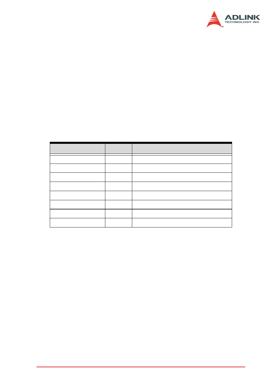
Address
R/W
Value Mapping (MSB----LSB)
BASE+0x16h
W
IDO[15...0]
BASE+0x18h
W
IDO[31...16]
BASE+0x1Ah
W
IDO[47...32]
BASE+0x1Ch
W
IDO[63...48]
BASE+0x1Eh
W
IDO[79...64]
BASE+0x20h
W
IDO[95...80]
BASE+0x22h
W
IDO[111...96]
BASE+0x24h
W
IDO[127...112]
Bit value:
0: Output PowerMOSFET is OFF. (Initial value)
1: Output PowerMOSFET is ON.