2 hardware information, 1 card layout, Card layout – ADLINK PCI-7442 User Manual
Page 21: 2hardware information
Hardware Information
9
2
Hardware Information
This chapter provides information on the PCI-7442/7443/7444
card layout, connectors, and pin assignments.
2.1
Card Layout
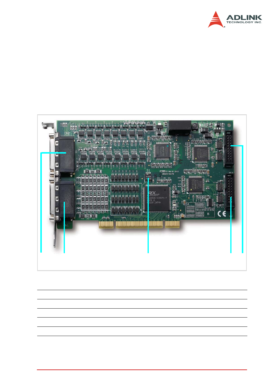
Figure 2-1 shows the location of the PCI-7442 connectors, switch,
and jumpers.
Figure 2-1: PCI-7442 Layout
1
CN2
64-CH isolated digital output connector
2
CN1
64-CH isolated digital input connector
3
S1
Board ID DIP switch
4
JP3
16-CH (TTL0~15) TTL I/O connector
5
JP4
16-CH (TTL15~31) TTL I/O connector
2
3
4 5
1