Data retention characteristics, Data retention waveform, Switching waveforms – Cypress CY7C1012DV33 User Manual
Page 6: Data retention waveform switching waveforms

CY7C1012DV33
Document Number: 38-05610 Rev. *D
Page 6 of 11
Data Retention Characteristics
Over the Operating Range
Parameter
Description
Conditions
[3]
Min
Typ
Max
Unit
V
DR
V
CC
for Data Retention
2
V
I
CCDR
Data Retention Current
V
CC
= 2V, CE > V
CC
– 0.2V,
V
IN
> V
CC
– 0.2V or V
IN
< 0.2V
25
mA
t
CDR
[11]
Chip Deselect to Data Retention
Time
0
ns
t
R
[12]
Operation Recovery Time
t
RC
ns
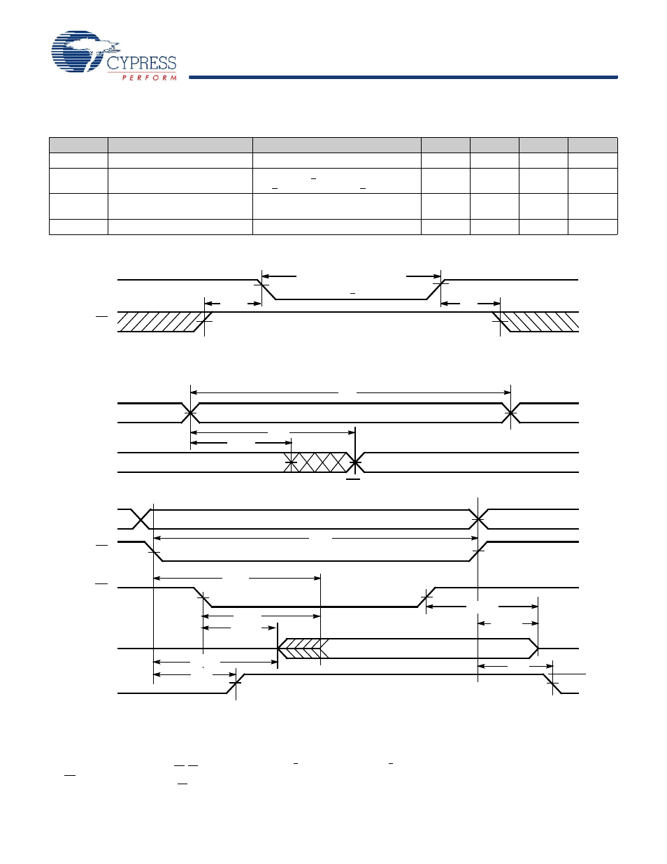
Data Retention Waveform
Switching Waveforms
Figure 3. Read Cycle No. 1
Figure 4. Read Cycle No. 2 (OE Controlled)
3.0V
3.0V
t
CDR
V
DR
>
2V
DATA RETENTION MODE
t
R
CE
V
CC
PREVIOUS DATA VALID
DATA VALID
RC
t
AA
t
OHA
t
RC
ADDRESS
DATA OUT
50%
50%
DATA VALID
t
RC
t
ACE
t
DOE
t
LZOE
t
LZCE
t
PU
HIGH IMPEDANCE
t
HZOE
t
PD
t
HZCE
OE
CE
ADDRESS
DATA OUT
V
CC
SUPPLY
CURRENT
HIGH
IMPEDANCE
I
CC
I
SB
Notes
11. Tested initially and after any design or process changes that may affect these parameters.
12. Full device operation requires linear V
CC
ramp from V
DR
to V
CC(min)
> 50
μs or stable at V
CC(min)
> 50
μs.
13. Device is continuously selected. OE, CE = V
IL
.
14. WE is HIGH for read cycle.
15. Address valid before or similar to CE transition LOW.
