4 controls for registers r1d to r23, Controls for registers r1d to r23 – Maxim Integrated 73M1966B User Manual
Page 15
UG_1x66B_002
73M1866B/73M1966B GUI User Guide
Rev. 1.1
15
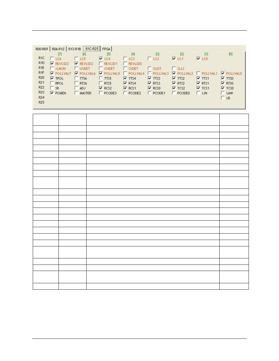
2.2.4 Controls for Registers R1D to R23
Registers
Description
Data Sheet
Section
R1C[7:1]
LCn
Loop Current
11.12
R1D[7:4]
REVLSDn
Line-Side Device Revision
7.1
R1E[7]
ILMON
Current Limit Mode On
10.6
R1E[6]
UVDET
Under-Voltage Detector
11.12
R1E[5]
OVDET
Over-Voltage Detector
11.12
R1E[4]
OIDET
Over-Current (I) Detector
11.12
R1E[3]
OLDET
Over-Load Detector
11.12
R1E[2]
SLLS
Synchronization Loss Line Side
9.5
R1F[7:0]
POLLVALn Polling Value
When polled, the content of the Line-Side Device Register
6.1
R20[7]
TPOL
Transmit Polarity
8.8
R20[6:0]
TTSn
Transmit Time Slot
8.8
R21[7]
RPOL
Receive Polarity
8.8
R21[6:0]
RTSn
Receive Time Slot
8.8
R22[7]
SR
Sampling Rate Mode
8.8
R22[6]
ADJ
Adjacent Time Slots
8.8
R22[5:3]
RCSn
Receive Clock Slot
8.8
R22[2:0]
TCSn
Transmit Clock Slot
8.8
R23[7]
PCMEN
PCM Transmit Enable
8.8
R23[6]
MASTER
Master/Slave Mode
0 = enables Slave Mode; 1 = enables Master Mode.
8.8
R23[5:2]
PCODEn
PCM Clock Code
8.8
R23[1]
LIN
Linear Mode Enable
8.8
R23[0]
LAW
Law Compression Mode
0 = selects A-
law; 1 = selects μ-law.
8.8
R24[0]
LB
Enables PCM Loopback within the Host-Side Device.
12.7