1 controls for registers r00 to r09, Controls for registers r00 to r09 – Maxim Integrated 73M1966B User Manual
Page 11
UG_1x66B_002
73M1866B/73M1966B GUI User Guide
Rev. 1.1
11
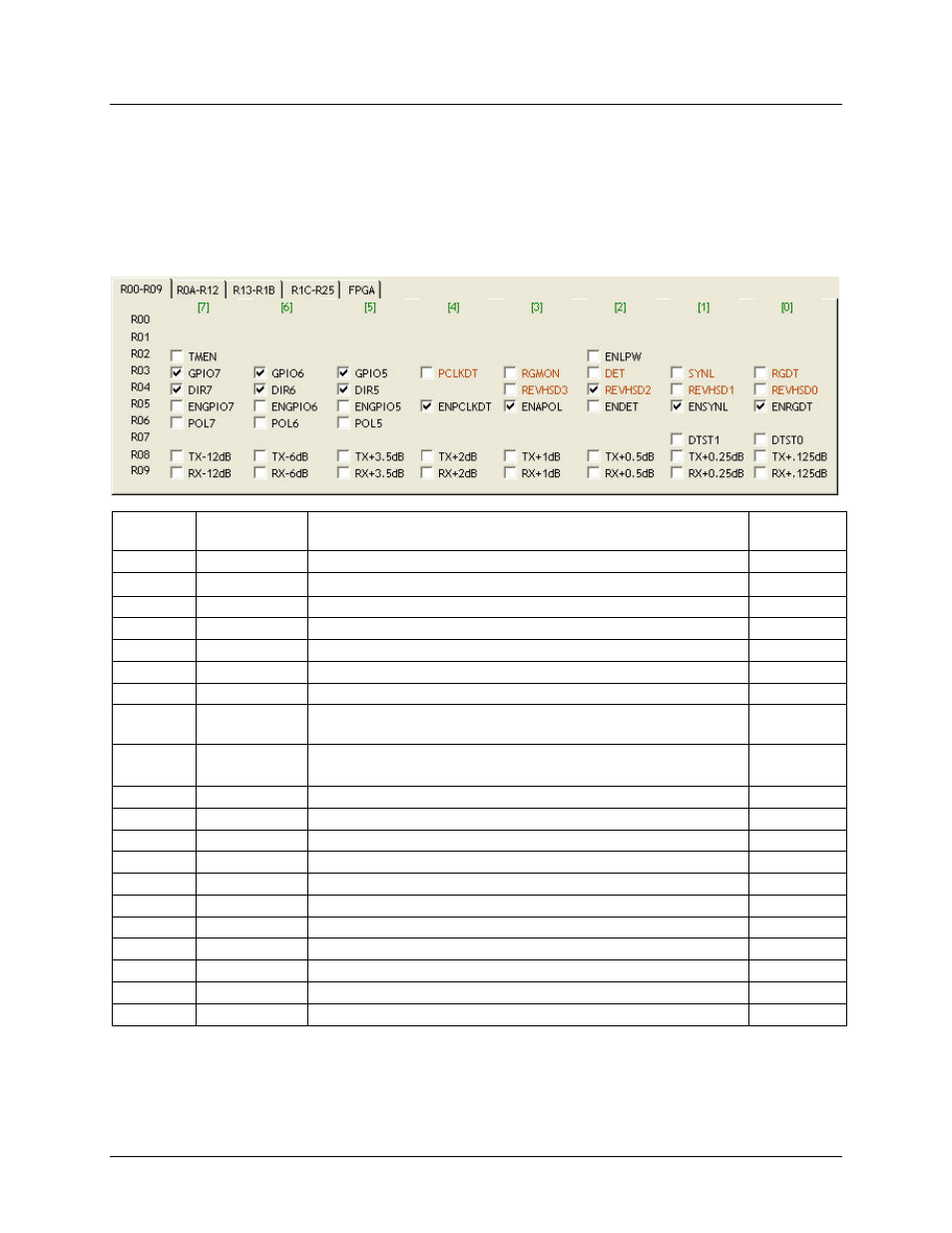
2.2.1 Controls for Registers R00 to R09
The GUI represents 73M1x66B registers in the form Rhh, where hh is the hexadecimal address. The
73M1866B/73M1966B Data Sheet represents these same registers in the form 0xhh.
For detailed descriptions of 73M1x66B registers, see the 73M1866B/73M1966B Data Sheet. The tables
below list the section numbers in the 73M1866B/73M1966B Data Sheet where additional information can
be found about each bit.
Register
Bit Name
Summary Description
Data Sheet
Section
R02[7]
TMEN
Test Mode Enable
12.7
R02[2]
ENLPW
Enable Line Power
9.5
R03[7:5]
GPIOn
GPIO Pin Enable
7.5
R03[4]
PCLKDT
PCLK Error Detected
8.8
R03[3]
RGMON
Ringing Monitor – 0 = silent, 1 = ringing
11.12
R03[2]
DET
Voltage Detection – 1 = detection of one of three conditions
11.12
R03[1]
SYNL
Barrier Synchronization Loss has occurred
9.5
R03[0]
RGDT
Ring or Line Reversal Detection – 1 = a Latched Ring or Line
Reversal Detection event
11.12
R04[7:5]
DIRn
GPIO Input/Output Select – 0 = GPIO pin is an output,
1 = GPIO pin an input
7.5
R04[3:0]
REVHSDn
Host-Side Device Revision
7.1
R05[7:5]
ENGPIOn
GPIO Enable
7.5
R05[4]
ENPCLKDT
Enable PCLK Detection
8.8
R05[3]
ENAPOL
Enable Automatic Polling
9.5
R05[2]
ENDET
Enable Voltage Detection
11.12
R05[1]
ENSYNL
Enable Synch Loss Detection
9.5
R05[0]
ENRGDT
Enable Ring Detection Interrupt
11.12
R06[7:5]
POLn
GPIO Interrupt Edge Selection
7.5
R07[1:0]
DTSTn
Digital Test Mode Select
12.7
R08
TXDGn
Transmitter Digital
8.8
R09
RXDGn
Receiver Digital Gain
8.8