Assembly instructions – ebm-papst VDC-3-49.15 User Manual
Page 6

VDC-3-49.15
Assembly instructions
Article No.: 194 0005 008 · Version: V1.0 · dated 08.11.2011 · Page 6 of 14
ebm-papst St. Georgen GmbH & Co. KG · Hermann-Papst-Straße 1 · 78112 St. Georgen · Phone: +49 7724 81-0 · Fax: +49 7724 81-1309 · www.ebmpapst.com · [email protected]
Ori
g
inal installation
Digital output signal "D" (yellow) – drive status
If certain errors and associated safety shut-offs of the drive occur, a low
signal (open collector) is output at output "D" as a fault-signal.
For a more detailed description of the corresponding protection functions,
refer to Chapter 5. The drive can only restart until after digital input "C" is
acknowledged (change of the signal level from 0 to 1).
NOTE
Output D is not short-circuit proof and has no reverse
polarity protection.
If the output is overloaded or incorrectly poled, this will damage
the output wiring.
Signals can no longer be evaluated.
Æ
Observe the information for max. voltage and current.
Design -
Open
collector
Max. external voltage
U
ext. max
V
≤ 36
Collector current
I
C
mA
1 < IC < 10
Saturation voltage
U
CEsat
V
0.4
Logic -
0 = Fault, drive inactive
1 = No fault, drive active
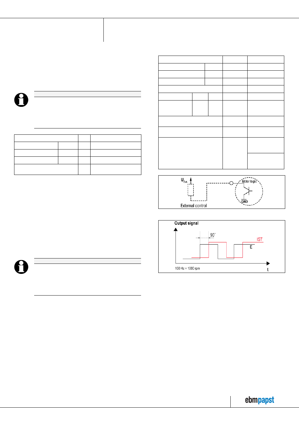
Digital output signals "E" (Channel A, red) and "IST" (Channel B, grey)
for information about speed and direction of rotation
Each of the two open collector outputs can be read out separately as actual
speed value information. A rectangular signal is present at both outputs, and
can be evaluated either as a frequency or as a number of pulses (e.g.
number of rising edges per revolution). By default, the frequency is defined
such that 6 pulses (signal periods) per revolution are output.
This results in the following relationship:
Signal frequency * 10 = speed in rpm.
For design variants that deviate from this, the information in the product
specification must be taken into account.
When evaluating both outputs, a 2-channel encoder replacement signal is
obtained; as a result, both the double speed information and the direction of
rotation can be identified via the assignment of the leading channel.
NOTE
Outputs E and IST are not short-circuit proof and have no
reverse polarity protection.
If the output is overloaded or incorrectly poled, this will damage
the output wiring.
Signals can no longer be evaluated.
Æ
Observe the information for max. voltage and current.
Design -
Open
collector
Max. external voltage
U
ext. max
V
36
Collector current
I
C
mA
1 < IC < 10
Saturation voltage
U
CEsat
V
0.4
Max. output frequency
kHz
1
Duty cycle
±2%
%
50
Phase offset
to Channel B
(IST)
±25 %
°
90
Output of speed information at "E"
or "IST"
Pulses per
revolution
6
Encoder replacement signal,
Channel A/B information
Pulses per
revolution
12
Direction of rotation assignment
Channel A leading
before Channel B =
cw
Channel B leading
before Channel A =
ccw
Fig.4 Schematic diagram of open collector output for E and IST
Fig.5 Rectangular signals at the outputs E and IST
