Digilent XCRP User Manual
Page 2
XCRP Reference Manual
Digilent, Inc.
Copyright Digilent, Inc.
Page 2/2
Doc: 502-046
devices. All CPLD signals are routed to an
expansion connector so that designs can
easily be extended using the on-board
solderless breadboard, or by attaching
accessory boards. The board can run on two
AA cells, so designs are portable. It includes a
XCR3064 CoolRunner CPLD, a JTAG
configuration circuit that uses a standard
parallel cable, a user-settable oscillator circuit,
and several useful I/O devices.
Table 1 shows all signals routed on the XCRP
board. These signals and their circuits are
described in the following sections.
CPLD configuration circuit
The XCRP board uses a JTAG port connector
to route programming signals from a host
computer to the CPLD. The programming
circuit simply connects the JTAG port pins
driven by the Xilinx CAD tools directly to the
CPLD programming pins, making the board
fully compatible with all Xilinx programming
tools. To configure the board from a computer
using the JTAG cable, ensure the circuit is
powered either by batteries or by an external
power supply. Before running Xilinx’s iMPACT
programmer tool to download a bit file, ensure
that the JTAG start-up clock is selected in the
“Generate Programming File” properties dialog
box. Attach the programming cable, and start
the iMPACT programmer. The board will be
auto-detected by the Xilinx software, and all
normal JTAG operations will be available.
Operations are available in a pull-down menu
made visible by right clicking on the device
graphic in the iMPACT programmer window.
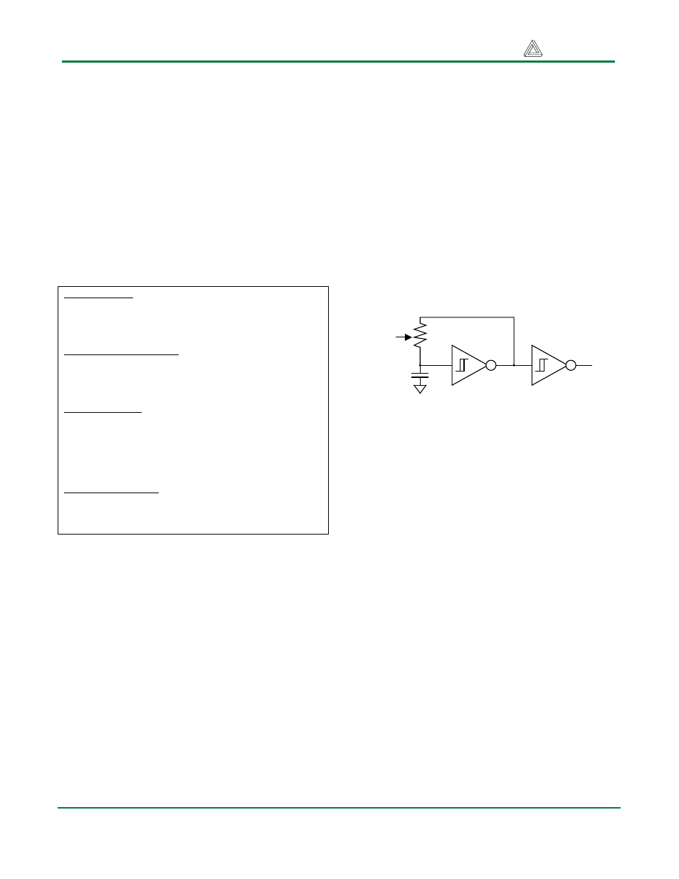
Oscillator
The XCRP board provides an user-adjustable
oscillator that can produce a clock signal in the
0.5 to 4KHz range. The oscillator circuit uses
an auto-feedback Schmidt-trigger inverter, with
a variable resistor and fixed 4.7uF capacitor in
the feedback path. The variable resistor is a
15-turn precision potentiometer that can be
adjusted from 0 to 500K ohms, providing an
RC time constant that varies by several orders
of magnitude. This clock source provides an
adequate frequency range for experiments that
run from “human time” (i.e., less than 1 Hz) to
the audio range. The oscillator output drives
the CLK0 input of the CPLD via a second
Schmidt trigger.
Power Supplies
The XCRP board can be powered from any
wall-plug transformer that uses a 2.1mm
center-positive jack, and that produces at least
100mA in the 5VDC to 9VDC range. The board
can also be powered from 2AA cells or any
other power source that outputs at least
100mA at 2.5 to 4.0 volts. The secondary
power source connector bypasses the on-
board regulators, so if that connector is used,
ensure that no more than 4VDC is applied to
the board. During operation, the board
Power Supplies
VBAT
Battery voltage
VEXT
External voltage applied to J4
VCC
System voltage (VBAT or VEXT)
GND
System ground routed to all devices
Programming parallel port
TDI
JTAG data input signal
TCK
JTAG clock signal
TMS
JTAG test mode select signal
TDO
JTAG data out signal
On board devices
MCLK
Master clock from user-settable oscillator
BTN1-4
Debounced button inputs
SW1-8
Slide switch inputs
LED1-8
Individual LED drive signals
CAT1, 2
Common cathode signals for 7Seg displays
AA-AG
Anode signals for seven segment displays
Expansion Connector
NA
All signals routed to connector (except MCLK)
Table 1. XCRP board signal definitions
MCLK
User
Adjust
Figure 2. Oscillator Circuit