Absolute maximum ratings, Dc operating characteristics, Ac operating characteristics – Digilent 210-203P-BOARD User Manual
Page 3
JTAG-SMT1 Programming Module for Xilinx® FPGAs
Copyright Digilent, Inc. All rights reserved.
Other product and company names mentioned may be trademarks of their respective owners.
Page 3 of 5
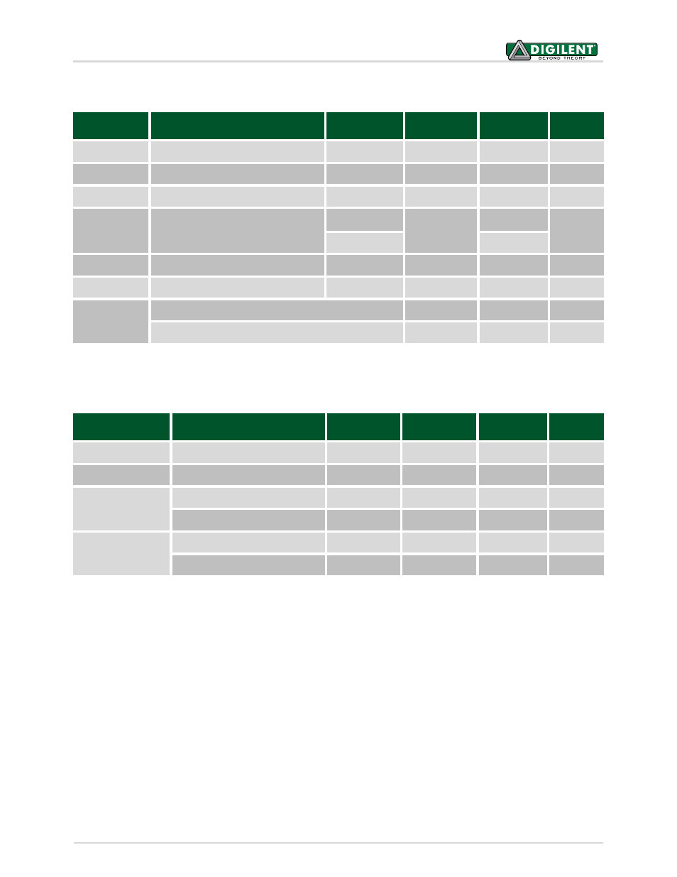
Absolute Maximum Ratings
Symbol
Parameter
Condition
Min
Max
Unit
Vdd
Operating supply voltage
-0.3
4.0
V
Vref
I/O reference/supply voltage
-0.3
6
V
VIO
Signal Voltage
-0.3
6
V
I
IK
,I
OK
TMS, TCK, TDI, TDO
DC Input/Output Diode Current
VIO < -0.3V
-50
mA
VIO > 6V
+20
I
OUT
DC Output Current
±50
mA
T
STG
Storage Temperature
-20
+120
ºC
ESD
Human Body Model JESD22-A114
2000
V
Charge Device Model JESD22-C101
500
V
DC Operating Characteristics
Symbol
Parameter
Min
Typ
Max
Unit
Vdd
Operating supply voltage
2.97
3.3
3.63
Volts
Vref
I/O reference/supply voltage
1.65
2.5/3.3
5.5
Volts
TDO
Input High Voltage (V
IH
)
0.75 x Vref
5.5
Volts
Input Low Voltage (V
IL
)
0
0.25 x Vref
Volts
TMS, TCK, TDI
Output High (V
OH
)
0.85 x Vdd
0.95 x Vdd
Vdd
Volts
Output Low (V
OL
)
0
0.05 x Vdd
0.15 x Vdd
Volts
AC Operating Characteristics
SMT1 JTAG signals are driven according to the timing diagram below. JTAG/TCK frequencies from 30 MHz to 8 KHz
are supported, at integer divisions of 30 MHz from 1 to 3750. Common frequencies include 30 MHz, 15 MHz, 10
MHz, 7.5 MHz, and 6 HMz. JTAG/TCK operating frequency can be set from within the Xilinx tools.
Note: Please refer to Xilinx’s iMPACT documentation for more information.