Digilent 210-203P-BOARD User Manual
Jtag-smt1 ™ programming module for xilinx, Fpgas, Overview
1300 Henley Court
Pullman, WA 99163
509.334.6306
www.digilentinc.com
JTAG-SMT1
™ Programming Module for Xilinx
®
FPGAs
Revised March 2, 2015
This manual applies to the JTAG-SMT1 rev. A
DOC#: 502-203
Copyright Digilent, Inc. All rights reserved.
Other product and company names mentioned may be trademarks of their respective owners.
Page 1 of 5
Overview
The JTAG-SMT1 is a compact, complete, and fully self-contained surface-mount programming module for Xilinx®
FPGAs. It can be accessed directly from all Xilinx Tools, including iMPACT, ChipScope™, and EDK. The module can
be loaded directly onto a target board and reflowed like any other component.
The JTAG-SMT1 uses a 3.3V main power supply and a separate Vref supply to drive the JTAG signals. All JTAG
signals use high speed, 24mA, three-state buffers that allow signal voltages from 1.8V to 5V and bus speeds of up
to 30MBit/sec. JTAG signals are actively driven only during a programming event and are otherwise held in high-
impedance, so the JTAG bus can be shared with other devices.
The SMT1 module is CE certified and fully compliant with the RoHS and REACH directives. It uses a standard Type-A
to Micro-USB cable, also available from Digilent.
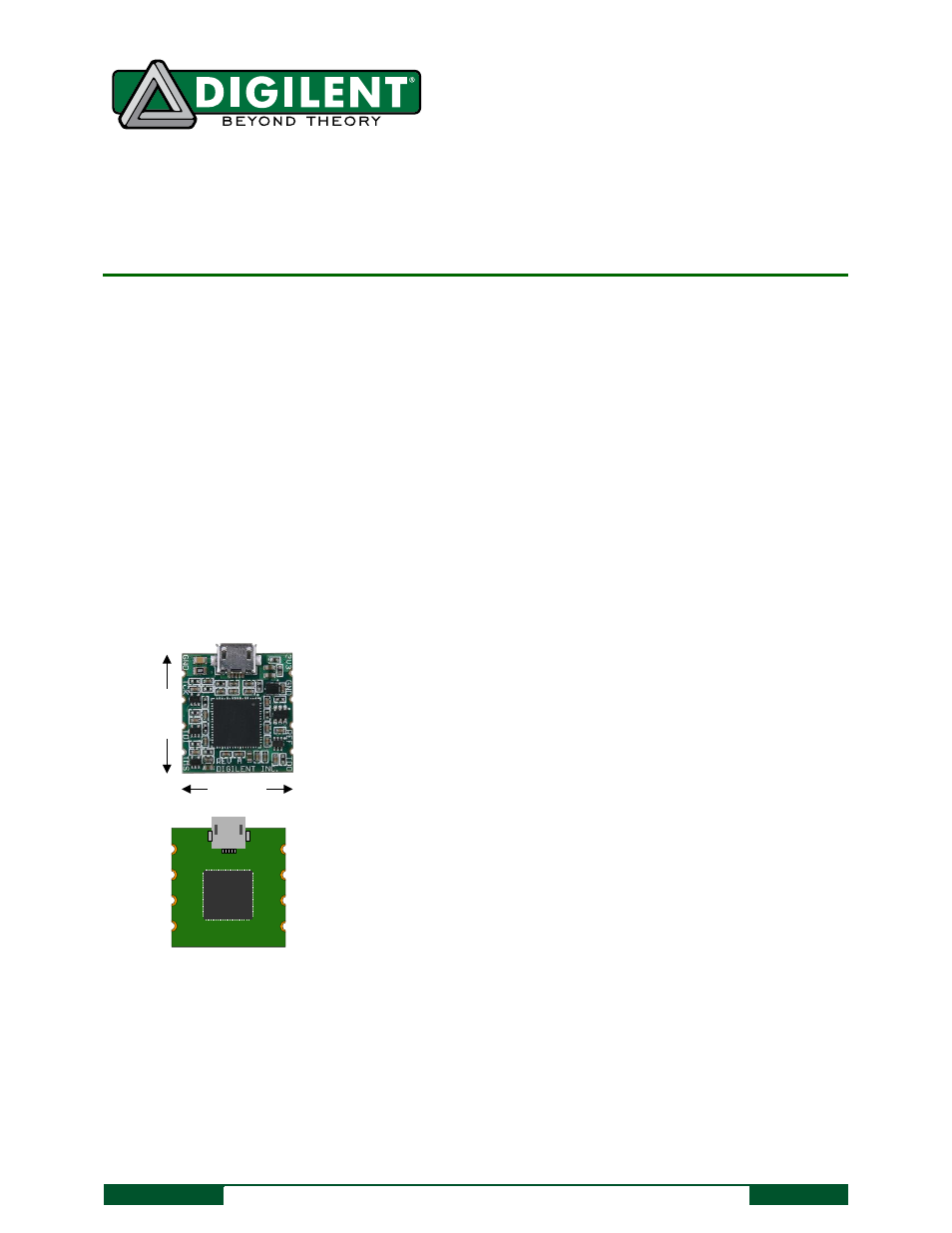
21.5mm
2
3
m
m
1
2
3
4
8
7
6
5
GND
TCK
TDI
TMS
Vdd (3.3V)
GND
VREF
TDO
The JTAG-SMT1.
Small, complete, all-in-one JTAG programming solution for
Xilinx FPGAs
Single 3.3V supply
Separate Vref drives JTAG signal voltages; Vref can be any
voltage between 1.8V and 5V.
High-Speed USB2 port that can drive JTAG/SPI bus at up to
30Mbit/sec
Able to drive JTAG bus at up to 30Mbit/sec
JTAG/TCK frequency settable by user
Compatible with all Xilinx tools
Small form-factor surface-mount module can be directly
loaded on target boards
Uses micro-AB USB2 connector
Same circuit is available as a stand-alone programming cable;
see Digilent’s JTAG-HS1.
The JTAG signals can be connected directly to the corresponding FPGA signals, as shown in the image below. For
best results, the module should be mounted adjacent to the edge of the host PCB over a ground plane. Although
signal traces may be run on top of the host PCB beneath the SMT1, it is recommended the area immediately
beneath the SMT1 be kept clear. For highest speed JTAG operation, impedance between the SMT1 and FPGA
should be kept below 100 Ohms.
Features include: