Terminal block interface, Standard specifications, Pin settings – KEYENCE XG-7000 Series User Manual
Page 6: Input/output circuit, Input circuit, Output circuit
6
Standard Specifications
The following values show the terminal block specifications for the system.
Tightening with a force above the standard torque may cause damage to the
terminal block.
OUT connector
• Socket block: MC1.5/9-ST-3.5BK
(Phoenix Contact)
• Compatible electric wires:
AWG16 to 28
• Terminal block screw torque:
0.25 Nm or less
IN connector
• Socket block: MC1.5/8-ST-3.5BK
(Phoenix Contact)
• Compatible electric wires:
AWG16 to 28
• Terminal block screw torque:
0.25 Nm or less
Pin Settings
OUT connector
• Power source 0 V and COMOUT1, COMOUT_F+, and COMOUT_F- are all
isolated.
• COMOUT1 is the common terminal for output terminals 1 and 2.
• COMOUT_F+ and COMOUT_F- are the common terminal for output
terminals 3, 4 and 6, 7.
IN connector
*1 Initial assignment status is a status that system variables are assigned to
the each terminal by the initial environment settings value. This may be
different from the original description due to setting change.
*2 For more details on the each variable function, see the "List of System
Variables" of XG VisionEditor reference manual.
• Power source 0 V and COMIN1 are all isolated.
• COMIN1 is the common terminal for input terminals 2 through to 6.
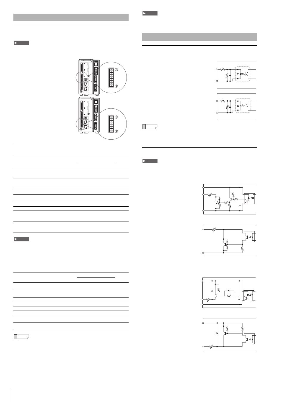
Input Circuit
Input circuit diagram
Circuit A (compatible with F_IN0 to 3, EV)
• Max. superimposed voltage: 26.4 V
• ON voltage: 10.8 V or greater
• ON current: 3 mA or greater
• OFF voltage: 5 V or less
• OFF current: 1 mA or less
Circuit B (other inputs)
• Max. superimposed voltage: 26.4 V
• ON voltage: 10.8 V or greater
• ON current: 2 mA or greater
• OFF voltage: 3 V or less
• OFF current: 0.3 mA or less
For more details on the common to be connected, see the "Parallel I/O
Interface" (page 5), and "Terminal Block Interface" (page 6).
Output Circuit
The working current of the Poly Switch for the over current is 1 A. Use the
current of 1 A or more for the output.
Output circuit diagram (NPN output type)
Circuit C (F_OUT0 to 3)
• Max. superimposed
voltage: 30 V
• Max. sink current:
50 mA
• Leakage current:
0.1 mA or less
• Residual voltage: 1.4 V or less (50 mA), 1.0 V or less (20 mA)
Circuit D (Other outputs)
• Max. superimposed
voltage: 30 V
• Max. sink current:
50 mA
• Leakage current:
0.1 mA or less
• Residual voltage: 1.4 V or less (50 mA), 1.0 V or less (20 mA)
Output circuit diagram (PNP output type, when the model has P
at the end of the name)
Circuit C (F_OUT0 to 3)
• Max. superimposed
voltage: 30 V
• Max. sink current:
50 mA
• Leakage current:
0.1 mA or less
• Residual voltage: 1.4 V or less (50 mA), 1.0 V or less (20 mA)
Circuit D (Other outputs)
• Max. superimposed
voltage: 30 V
• Max. sink current:
50 mA
• Leakage current:
0.1 mA or less
• Residual voltage: 1.4 V or less (50 mA), 1.0 V or less (20 mA)
Terminal Block Interface
No.
Name
Terminal ID is noted in ( )
Reference
Initial assignment status
*1
Circuit
diagram
Variable function
*2
Bit
1
(STO) OUT22
Output 22
I/O terminal/
Parallel I/O output
change strobe
0
D
2
(OR) OUT23
Output 23
Outputs the total
status output
0
D
3
(ERR) F_OUT2
High speed output 2
Error 0 output
0
C
4
(RUN) F_OUT3
High speed output 3
Run mode output
0
C
5
(COMOUT)
COMOUT1
Common for terminal
block outputs (1, 2)
–
–
–
6
(FLS1) F_OUT0
High speed output 0
Strobe output 1
0
C
7
(FLS2) F_OUT1
High speed output 1
Strobe output 2
0
C
8
(COMF+)
COMOUT_F+
Common for high
speed output (+)
(3, 4 and 6, 7)
–
–
–
9
(COMF-)
COMOUT_F-
Common for high
speed output (-)
(3, 4 and 6, 7)
–
–
–
No.
Name
Terminal ID is noted in ( )
Reference
Initial assignment status
*1
Circuit
diagram
Variable function
*2
Bit
1
(COMIN) COMIN1
Common for terminal
block inputs
–
–
–
2
(PLC) IN15
Input 15
Custom command
execution input (PLC)
0
B
3
(TRG1) F_IN0
High speed input 0
Trigger 1 input
0
A
4
(TRG2) F_IN1
High speed input 1
Trigger 2 input
0
A
5
(TEST) F_IN2
High speed input 2
Test run input
0
A
6
(EXT) F_IN3
High speed input 3
Disable trigger input
0
A
7
24 VDC
+ power supply (24
VDC) input
–
–
–
8
0 V
- power supply (0 V)
input
–
–
–
Note
Note
Reference
Input/Output Circuit
Note
INPUT
COMIN1
3.9 k
Ω
680
Ω
INPUT
COMIN1
or
COMIN2
6.2 k
Ω
4.7 k
Ω
Reference
Note
10 k
Ω
22 k
Ω
22 k
Ω
22 k
Ω
22 k
Ω
40 V
104
COMOUT_F+
COMOUT_F–
OUTPUT
0.3 A
Poly Switch
10 k
Ω
1 k
Ω
40 V
0.3 A
COMOUT
OUTPUT
Poly Switch
10 k
Ω
22k
Ω
33 V
104
COMOUT_F+
COMOUT_F–
OUTPUT
0.3 A
Poly Switch
10 k
Ω
1 k
Ω
33 V
0.3 A
OUTPUT
Poly Switch
COMOUT