Switching waveforms – Cypress CY7C145 User Manual
Page 9

CY7C145, CY7C144
Document #: 38-06034 Rev. *D
Page 9 of 21
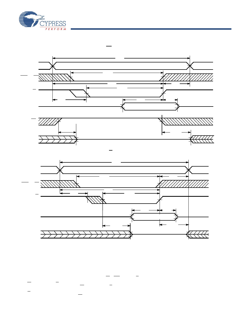
Figure 8. Write Cycle No. 1: OE Three-State Data I/Os (Either Port)
Figure 9. Write Cycle No. 2: R/W Three-State Data I/Os (Either Port)
Notes
21. The internal write time of the memory is defined by the overlap of CE or SEM LOW and R/W LOW. Both signals must be LOW to initiate a write, and either signal
can terminate a write by going HIGH. The data input set-up and hold timing should be referenced to the rising edge of the signal that terminates the write.
22. If OE is LOW during a R/W controlled write cycle, the write pulse width must be the larger of t
PWE
or (t
HZWE
+ t
SD
) to allow the I/O drivers to turn off and data to
be placed on the bus for the required t
SD
. If OE is HIGH during a R/W controlled write cycle (as in this example), this requirement does not apply and the write
pulse can be as short as the specified t
PWE
.
23. R/W must be HIGH during all address transitions.
24. Data I/O pins enter high impedance when OE is held LOW during write.
Switching Waveforms
(continued)
t
AW
t
WC
DATA VALID
HIGH IMPEDANCE
t
SCE
t
SA
t
PWE
t
HD
t
SD
t
HA
t
HZOE
t
LZOE
SEM OR CE
R/W
ADDRESS
OE
DATA OUT
DATA IN
t
AW
t
WC
t
SCE
t
SA
t
PWE
t
HD
t
SD
t
HZWE
t
HA
HIGH IMPEDANCE
SEM OR CE
R/W
ADDRESS
DATA OUT
DATA IN
t
LZWE
DATAVALID
