Switching characteristics – Cypress CY7C145 User Manual
Page 6

CY7C145, CY7C144
Document #: 38-06034 Rev. *D
Page 6 of 21
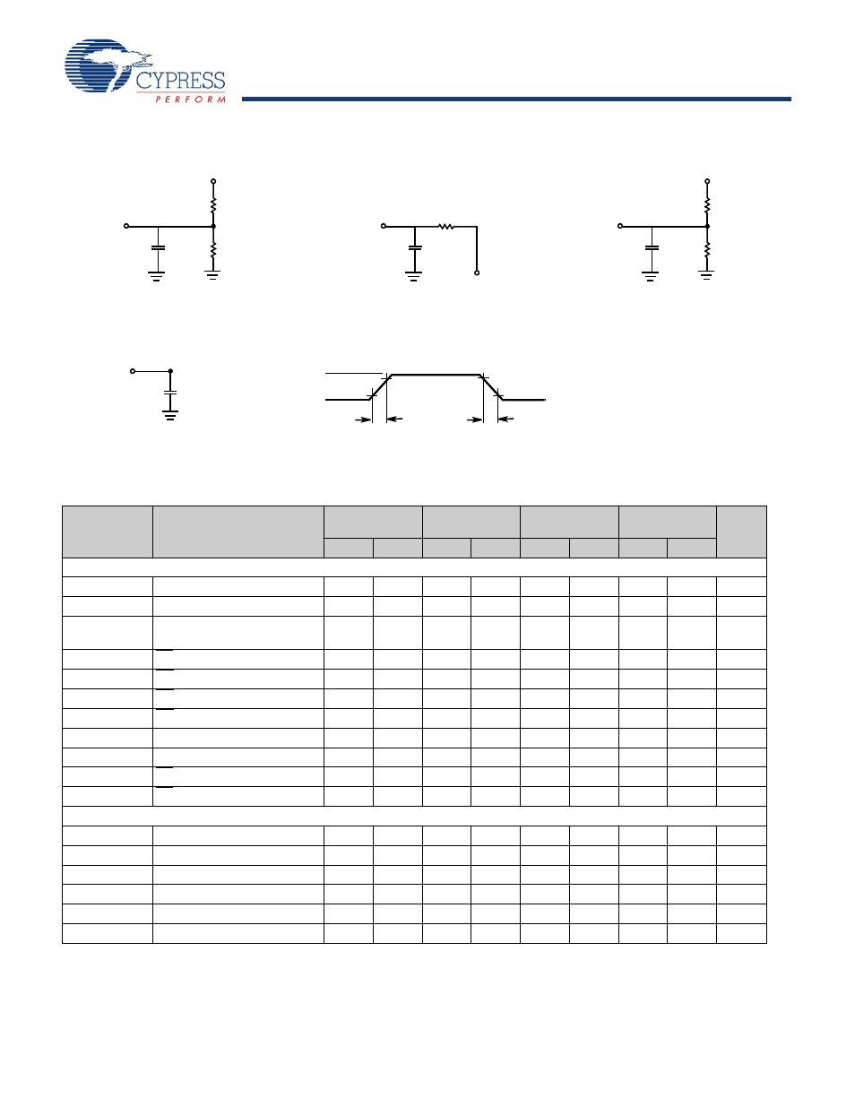
Figure 4. AC Test Loads and Waveforms
3.0V
GND
90%
90%
10%
≤ 3 ns
≤ 3 ns
10%
ALL INPUT PULSES
(a) Normal Load (Load1)
5V
OUTPUT
C = 30 pF
V
TH
= 1.4V
OUTPUT
C = 30pF
(b) Th évenin Equivalent (Load 1)
(c) Three-State Delay (Load 3)
C = 30 pF
OUTPUT
Load (Load 2)
5V
OUTPUT
C = 5 pF
R1 = 893
Ω
R2 = 347
Ω
R
TH
= 250
Ω
R1 = 893
Ω
R = 347
Ω
Switching Characteristics
Over the Operating Range
Parameter
Description
7C144-15
7C145-15
7C144-25
7C145-25
7C144-35
7C145-35
7C144-55
7C145-55
Unit
Min
Max
Min
Max
Min
Max
Min
Max
READ CYCLE
t
RC
Read Cycle Time
15
25
35
55
ns
t
AA
Address to Data Valid
15
25
35
55
ns
t
OHA
Output Hold From Address
Change
3
3
3
3
ns
t
ACE
CE LOW to Data Valid
15
25
35
55
ns
t
DOE
OE LOW to Data Valid
10
15
20
25
ns
t
LZOE
OE Low to Low Z
3
3
3
3
ns
t
HZOE
OE HIGH to High Z
10
15
20
25
ns
t
LZCE
CE LOW to Low Z
3
3
3
3
ns
t
HZCE
CE HIGH to High Z
10
15
20
25
ns
t
PU
[12]
CE LOW to Power-Up
0
0
0
0
ns
t
PD
[12]
CE HIGH to Power-Down
15
25
35
55
ns
WRITE CYCLE
t
WC
Write Cycle Time
15
25
35
55
ns
t
SCE
CE LOW to Write End
12
20
30
45
ns
t
AW
Address Set-Up to Write End
12
20
30
45
ns
t
HA
Address Hold From Write End
2
2
2
2
ns
t
SA
Address Set-Up to Write Start
0
0
0
0
ns
t
PWE
Write Pulse Width
12
20
25
40
ns
Notes
9. Test conditions assume signal transition time of 3 ns or less, timing reference levels of 1.5V, input pulse levels of 0 to 3.0V, and output loading of the specified
I
OI
/I
OH
and 30-pF load capacitance.
10. At any given temperature and voltage condition for any given device, t
HZCE
is less than t
LZCE
and t
HZOE
is less than t
LZOE
.
11. Test conditions used are Load 3.
12. This parameter is guaranteed but not tested.
