Assembly options, Assembly procedure – Elecraft AT1 41 dB Step Attenuator User Manual
Page 2
2
Reference. Designator
Description
Qty
Part
Number
R8 18
Ω (180) 1W Resistor
1
E500259
R10, R12
150
Ω 2W Resistor
2
E500260
R11 39
Ω (390) 2W Resistor
1
E500261
R13, R15
100
Ω 2W Resistor
2
E500262
R14 68
Ω 2W Resistor
1
E500078
R16, R18
62
Ω 2W Resistor
2
E500167
R17 240
Ω 2W Resistor
1
E500263
SW1, SW2, SW3, SW4, SW5, SW6
Slide Switch
6
E640032
Misc.
Wooden Spacer (see Figure 2 on page 3).
1
E980131
Misc. Rubber
Foot
4
E700024
Assembly Options
The AT1 is designed to operate as a stand-alone unit without an enclosure. Options are provided in case you want to build the
unit into an enclosure or existing equipment:
1. Your AT1 is provided with BNC connectors that mount parallel to the board. Normally these connectors will be
mounted on the top (silk screened) side of the board so that the board rests flat on the supplied rubber feet attached
to the bottom. However, if you are building the unit to place in an enclosure of your choice, you may elect to mount
the BNC connectors on the bottom of the board so the switches can be flush with the enclosure cover. Also, you may
purchase right-angle BNC connectors that may be mounted either on the top or the bottom of the board. Suitable
connectors are available from Digi-Key
®
(
www.digikey.com
, part number A32246-ND) or Mouser Electronics
®
(
www.mouser.com
, part number 571-2272226).
2. Four holes are provided in the board that you may use with your own #4 hardware and spacers as needed to mount
the unit instead of using the rubber feet.
Assembly Procedure
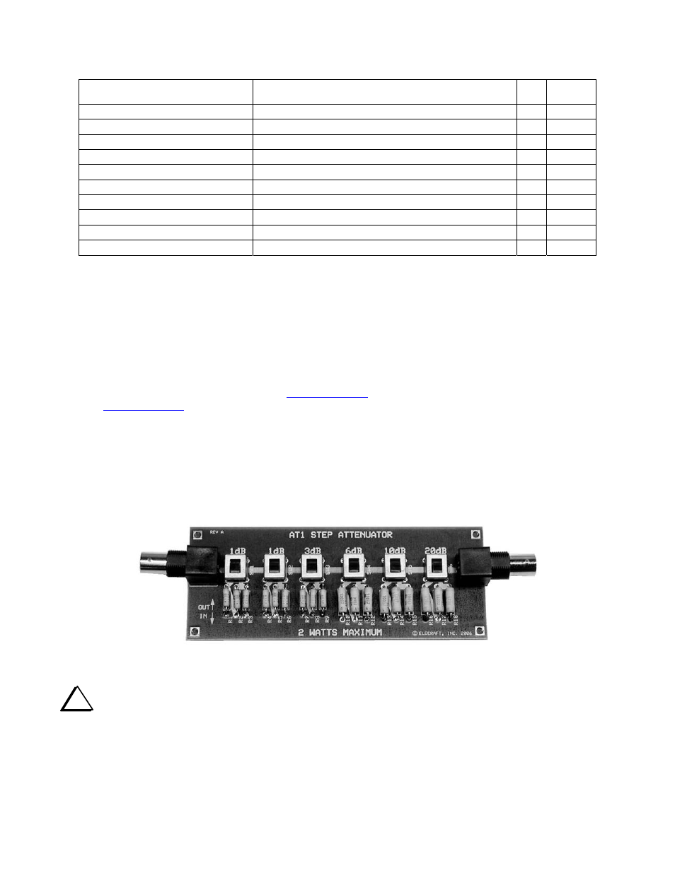
The finished Attenuator is shown in Figure 1. We recommend you follow the assembly procedure below, and refer to this
figure as needed.
Figure 1. Assembled AT1 Step Attenuator.
i
Use adequate ventilation when soldering; avoid inhaling smoke or fumes. Always wash your hands after
handling solder, as lead residue is highly toxic.
When applying solder, use the minimum amount required to surround the component lead and make good contact with its
printed-circuit pad. You don't need a "fillet" (build-up) of solder. This will avoid unwanted solder bridges and any need to
clean the PC boards.
The solder must flow onto both the component lead and its PC board pad. To ensure that both will be heated at the same time,
the tip of the iron should contact both the component lead and the PC board pad before solder is applied.