Achronix Speedster22i Pin Connections and Power Sequencing User Manual
Page 6

6
UG042, August 19, 2014
command and programming commands are sent via control
registers writes done via the IEEE 1149.1 JTAG interface. In
the CPU mode, this pin is the bidirectional data bit 0, DQ[0]
unconnected.
CSN[3:0]
CFG
Input /
Output
In SPI Mode: The CSN[3:0] pins are active-low chip select
outputs. In the programming mode, individual serial flash
devices are mapped to a linear addressing space. In the SPI x1
configuration mode only the CSN[0] output is used.
In CPU Mode: CSN[3] is the bidirectional data bit 6, DQ[6].
CSN[2] is the bidirectional data bit 7, DQ[7]. CSN[1] is not
used. CSN[0] is an active-low chip select input.
For SPI Mode: If SPIx1 is used, leave
CSN[3:1] unconnected. In SPIx4, connect all
four to the individual serial flash devices.
For CPU Mode: Connect CSN[3], CSN[2] and
CSN[0] directly to the configuration
controller. Tie CSN[1] to GND.
SD[3:0]
CFG
Input
Input pins providing data input from the flash device(s). In SPI
x4 configuration mode, all 4 SD inputs are utilized. When in
SPI x1 mode, only the SD[0] input is used to input the
configuration data. In the CPU mode, these bits serve as the
bidirectional data bits 1 through 4 (SD3=DQ1, SD2=DQ2,
SD1=DQ3, SD0=DQ4)
Connect directly to the configuration
controller. Do not leave these pins
unconnected.
CONFIG_SYS_CLK_BYPASS
CFG
Input
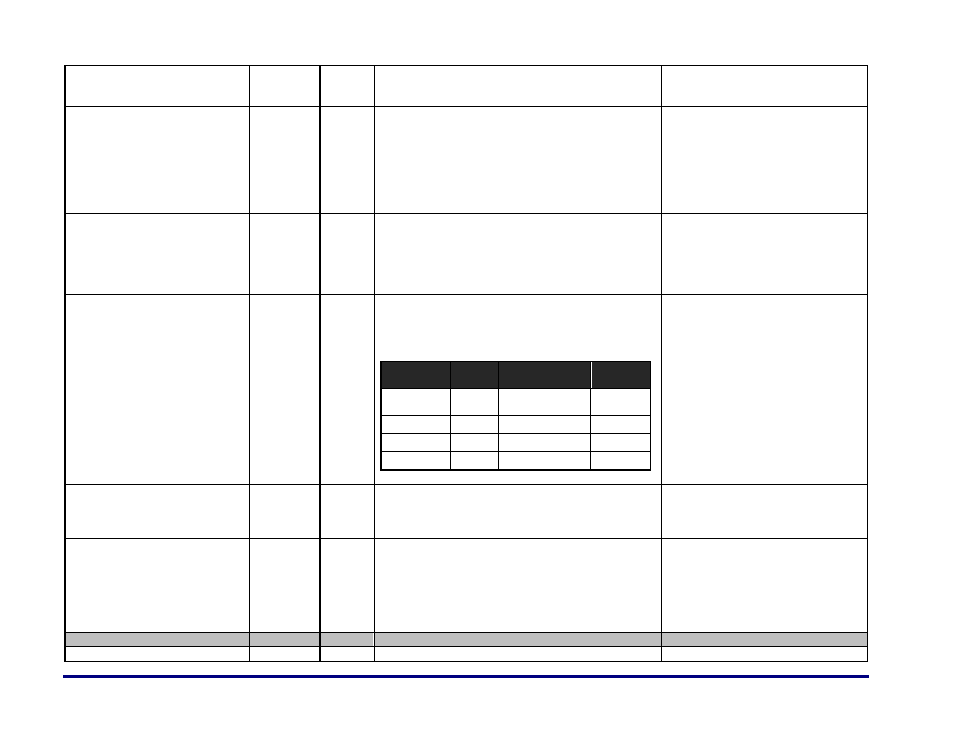
Pin statically enabling the bypass of the internal SYS_CLK. The
default clock for the FPGA configuration unit (FCU) is named
SYS_CLK. An on-chip ring oscillator (~10MHz) is the source for
SYS_CLK. For debug purposes this clock can be bypassed and
an external clock supplied.
CONFIG_SYS_
CLK_BYPASS
CONFIG_
CLKSEL
CONFIG_MODESEL
[2:0]
FCU CLK
0
0
001, 010
On-chip
oscillator
1
0
001, 010
CPU_CLK
0/1
0
100
CPU_CLK
0
1
000, 001, 010, 100
TCK
Do not leave this pin unconnected. It
should be connected to a configurable
input like a DIP switch to toggle between
modes of operation for debug. If this is not
possible or desired, tie this off to 1.8V
(VDDO_JCFG / PA_VDD2) or GND based on
the desired clock for the configuration
mode.
START_CFG_STARTUP
CFG
Input
Used to restart the configuration startup state machine after
the startup is already complete. This option is used if any
errors are encountered in the configuration memory from
ECC. NOT Available for HD1000.
For the HD1000 tie this pin to GND. For
other devices, connect this pin directly to
the configuration controller.
STAP_SEL
CFG
Input
When asserted high, this allows the JTAG interface pins to be
directly connected to the JTAG controller in Serdes PMA
blocks allowing SerDes configuration, debug and performance
monitoring directly from the JTAG interface. For bitstream
download and chip debug using the JTAG interface, this pin
must be held low. For SerDes PMA debug only mode, this pin
must be held high.
Do not leave this pin unconnected. It
should be connected to a configurable
input like a DIP switch to toggle between
modes of operation for debug.
READ_STATE_ERR
CFG
Output
Debug output signal in fabric testing.
Leave unconnected.
CONFIG_SCRUB_MULTIPLE_ERR
CFG
Output
Indicates the presence of multiple errors when the SCRUB
For the HD1000, leave unconnected. For
