Achronix Speedster22i Pin Connections and Power Sequencing User Manual
Page 10
10
UG042, August 19, 2014
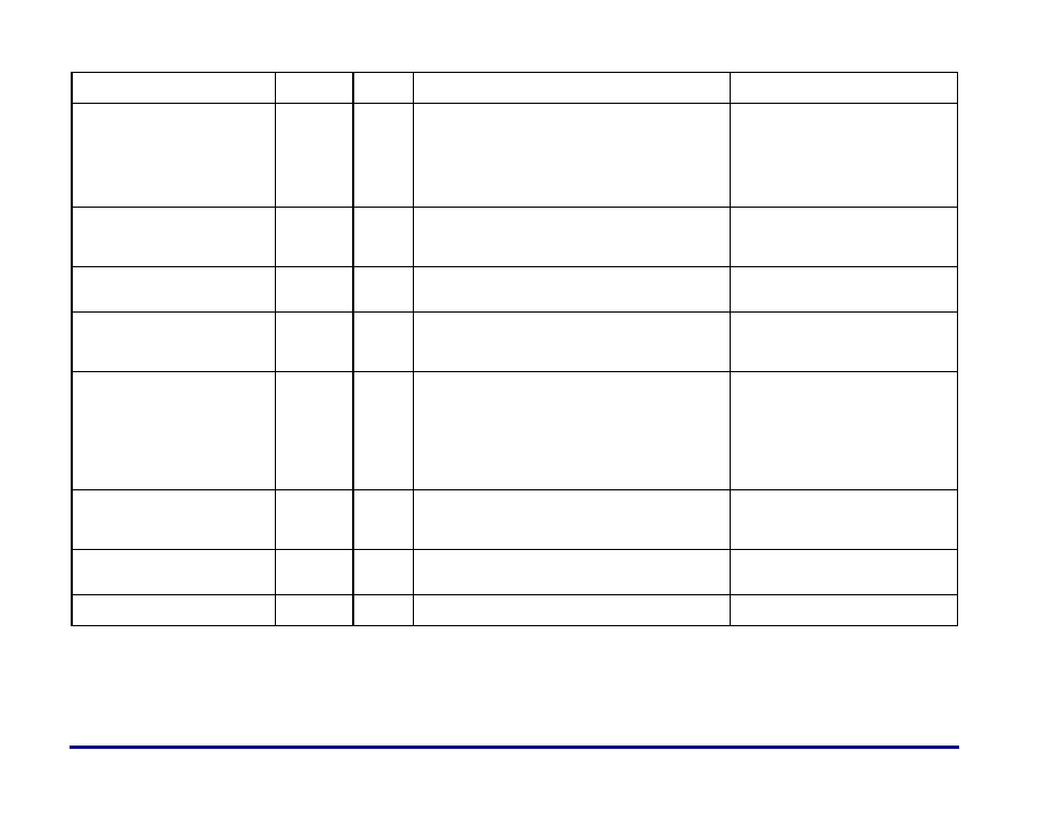
the FPGA fabric.
regulator. This supply can be shared with
VCC and VDD_BRAM.
VDD_CFGWL
CFG
Power
Power Supply for the wordlines of the configuration memory
SRAM cells in the FPGA fabric.
For configuration memory readback
capability (primarily for debug purposes),
this supply would need to be set to 0.9V
using a separate regulator. If this capability
is not needed or desired, this supply can be
more simply set to 1.0V and shared with
VDD_CFG, VCC and VDD_BRAM.
VDDA_NOM_W
WVDDA
Power
Analog Power Supply for FPGA circuitry in the I/O ring.
Connect VDDA_NOM_W to a 1.0V linear
regulator. The only 1.0V supplies that can
be shared with this supply are the eFuse
power supplies.
VDD_BRAM
VDD_BRAM
Power
Power Supply for Block RAMS in Fabric.
Connect VDD_BRAM to a 1.0V linear
regulator. This supply can be shared with
VCC and VDD_CFG.
VREF_B[00,01,02,10,11,12,20,21,22,
30, 31,32,40,41,42,50,51,52]
VDD_BANK
Power
Analog input; Voltage Bias reference. Half of corresponding
bank / cluster voltage level.
Connect to a biasing circuit like a
termination regulator with a reference
based on the corresponding I/O cluster's
power supply.
VDDO_B[00,01,02,10,11,12,20,21,22,
30, 31,32,40,41,42,50,51,52]
VDD_BANK
Power
Bank I/O supply voltage. An I/O bank is defined as a group of
byte-lanes that have a common power ball eg. 00. 3 I/O banks
make up an I/O cluster eg. 00, 01, 02. x0 and x1 I/O banks
have 4 byte lanes each and x2 I/O banks have 5 byte lanes to
give a total of 13 byte-lanes or (13x12) 156 I/O pins.
Note: Even though each I/O bank has a separate power ball,
all 3 I/O banks in the I/O cluster are required to be set to the
same voltage due to internal power rail sharing.
The I/O supply voltage can be set to 1.2V,
1.5V or 1.8V. The I/O standard can be
configured at a single I/O pin granularity,
but because all I/Os in the same I/O cluster
share a common supply, the standards
need to be voltage compatible.
VREF_CLK_BANK_[SE, SW, NE, NW]
VDD_BANK
Power
Analog input; Voltage Bias reference for clock banks. Half of
corresponding bank voltage level.
Connect to a biasing circuit like a
termination regulator with a reference
based on the corresponding clock bank's
power supply.
VDDO_CB[SE, SW, NE, NW]
VDD_BANK
Power
Clock bank I/O supply voltage
The I/O supply voltage can be set to 1.2V,
1.5V or 1.8V. The I/O standard can be
configured at clock bank corner granularity.
VSS
VSS
Power
Ground
All GND pins should be connected to the
board ground plane.