Achronix Speedster22i Pin Connections and Power Sequencing User Manual
Page 5
UG042, August 19, 2014
5
PROGRAM_ENABLE[1:0]
CFG
Input
Pin enabling the programming of the eFuse for the AES
encryption keys, which is done in the manufacturing and
testing of the devices. These input pins will not be usable by
customers.
Tie to GND.
CONFIG_DONE
CFG
Input
with
open-
drain or
active
output
Pin pulled low by FCU prior to the completion of device
configuration. After the device successfully completes
configuration, this pin is either tri-stated or can optionally be
driven high. The default behavior is open-drain, tri-stating the
pin when the device is properly configured. If a device
configuration error occurs, the CONFIG_DONE output for the
device remains in low. The device does not enter the
functional mode until this pin is high. Holding this pin low on
the board can be used as a method to synchronize the start-
up of multiple devices.
In the default mode of operation, it is
recommended that this signal be
connected to an LED as an indicator on the
board. In this case, use an external 10-kΩ
+/- 5% pull-up resistor to 3.3V and drive a
1-kΩ resistor to the input of a FET to turn
on the LED. If LED usage is not desired, this
signal can be pulled-up to 1.8V
(VDDO_JCFG / PA_VDD2) instead using the
same 10-kΩ pull-up resistor.
CONFIG_CLKSEL
CFG
Input
Pin controlling whether the FCU clock is sourced from the TCK
input or the CPU_CLK input.
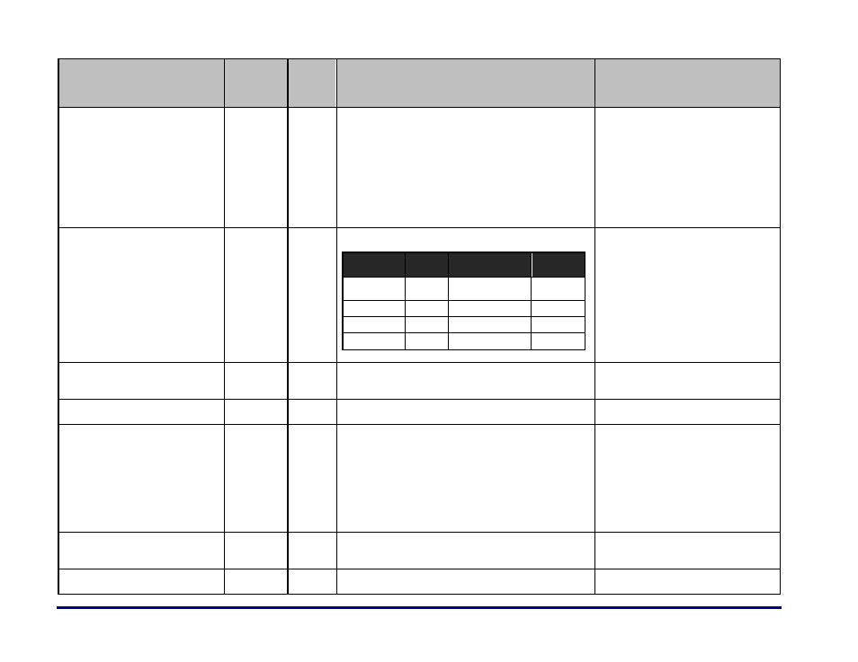
CONFIG_SYS_
CLK_BYPASS
CONFIG_
CLKSEL
CONFIG_MODESEL
[2:0]
FCU CLK
0
0
001, 010
On-chip
oscillator
1
0
001, 010
CPU_CLK
0/1
0
100
CPU_CLK
0
1
000, 001, 010, 100
TCK
Do not leave this pin unconnected. It
should be connected to a configurable
input like a DIP switch to toggle between
modes of operation for debug. If this is not
possible or desired, tie this off to 1.8V
(VDDO_JCFG / PA_VDD2) or GND based on
the desired clock for the configuration
mode.
HOLDN
CFG
Input /
Output
In the SPI mode of operation, the hold signal output for SPI
flash devices. In CPU mode, this bit is the bidirectional data
bit 5, DQ[5].
Connect directly to the configuration
controller. Do not leave this pin
unconnected.
CPU_CLK
CFG
Clock
Maximum 25Mhz. Used as FCU clock under CONFIG_CLKSEL
control.
If the CPU_CLK is not used to source the
FCU clock, then pin should be tied to GND.
BYPASS_CLR_MEM
CFG
Input
Input to enable bypassing of the configuration memory
clearing before device configuration.
Do not leave this pin unconnected. It
should be connected to a configurable
input like a DIP switch, or even dynamically
controlled through the configuration
controller. This will enable toggling
between modes of operation for debug and
may help with re-configuration time
optimization. If this is not possible or
desired, this pin should be tied to GND.
SCK
CFG
Output
Serial flash clock output. Clock can be sourced from either
CPU_CLK (user driven) or on-chip oscillator (~10MHz).
For SPI Mode: Connect directly to the flash
device(s).
For CPU Mode: Leave unconnected.
SDI
CFG
Input /
Output
In the SPI modes of operation, the serial data output pins for
command and programming data to the flash memory. These
Connect directly to the configuration
controller. Do not leave this pin