Power supplies and sequencing, Power supply block diagram – Achronix Speedster22i Pin Connections and Power Sequencing User Manual
Page 11
UG042, August 19, 2014
11
Power Supplies and Sequencing
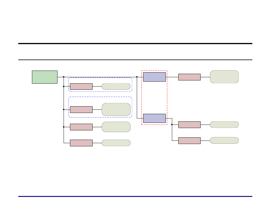
Power Supply Block Diagram
12V DC Board
Supply
Pre-Switching
Regulator
Regulator
Regulator
VDDL
1.0V
VCC
VDD_CFG
VDD_BRAM
VDD_CFGWL**
1.0V
Regulator
VDDA_NOM_E/W
VCCRAM_EFUSE[3:1]
VCCFHV_EFUSE[3:1]***
1.0V
Regulator
VDDO_B[xx]
VDDO_CB[xx]
1.2V /
1.5V /
1.8V
Pre-Switching
Regulator
Regulator
PA_VDD1
PA_VREG_CMN
PA_VREG_RX
PA_VREG_SYNTHX
0.95V
Regulator
PA_VDD2
VDDO_JCFG*
Regulator
AVDD_PLL
1.8V
1.7V
Helps with voltage
stability for
voltage sensitive
supplies
* It is preferable to share VDDO_JCFG with a voltage compatibale VDDO_B[xx] supply if a 1.8V IO Standard is being used in the design.
** For reliable configuration memory readback capability (primarily for debug), VDD_CFGWL needs to be set to 0.9V. Use a separate regulator to implement this.
If readback capability is not desired, or if this implementation is not possible, VDD_CFGWL can be set to 1.0V.
*** For applications requiring the blowing of fuses (eg. encryption keys for design security), VCCFHV_EFUSE[3:1] must be powered by a separate regulator
capable of providing voltages in the 1.0V
– 2.2V range. Refer to the Design Security section of the Configuration User Guide UG033 for implementation details.
Sense line feedback needed for regulator ****
Sense line feedback needed for regulator ****
**** For these supplies with higher static and dynamic current needs, sense lines are needed to ensure that feedback is provided to the regulators to compensate for
IR drops in the system. For the VCC / VDD_BRAM / VDD_CFG / VDD_CFGWL supply, voltage sensing on the VCC and VDD_BRAM supplies is most critical.