Achronix Speedster22i Pin Connections and Power Sequencing User Manual
Page 4
4
UG042, August 19, 2014
IEEE1149.1 JTAG Interface
Do not leave JTAG I/Os unconnected. The
JTAG interface should be brought out to a
JTAG header on the board.
TMS
JTAG
Input
Test Mode Select (TMS) input controlling the test access port
(TAP) controller state machine transitions. This input is
captured on the rising edge of the test logic clock (TCK).
This dedicated pin is equipped with an
internal pull-up resistor to place the test
logic in the Test-Logic-Reset state. Connect
this pin using a 10-kΩ +/- 5% pull-up
resistor to VDDO_JCFG (1.8V).
TCK
JTAG
Input
Dedicated test clock used to advance the TAP controller and
clock in data on TDI input and out on TDO output. The
maximum frequency for TCK is 100 MHz.
Connect this pin using a 1-kΩ +/- 1% pull-
down resistor to GND.
TDI
JTAG
Input
Serial input for instruction and test data. Data is captured on
the rising edge of the test logic clock.
Dedicated pin with an internal pull-up
resistor. Connect this pin using a 10-kΩ +/-
5% pull-up resistor to VDDO_JCFG (1.8V).
TRSTN
JTAG
Input
Active-low reset input used to initialize the TAP controller.
Dedicated pin and an optional port on
some devices. Connect this pin using a 4.7-
kΩ +/- 5% pull-down resistor to GND.
TDO
JTAG
Output
Serial output for data from the test logic. TDO is set to an
inactive drive state (high impedance) when data scanning is
not in progress. TDO drives out valid data on the falling edge
of the TCK input.
Use a 10-kΩ +/- 5% pull-up resistor to
VDDO_JCFG (1.8V) to minimize leakage in
the TDI input buffer of interfacing devices.
Configuration Interface
CONFIG_STATUS
CFG
Open
drain
output
Signal from open-drain output pulled low by FCU until the
configuration memory is successfully cleared. After this, I/O is
tri-stated and the external pull-up should pull this signal high.
It is recommended to connect this signal to
an LED as an indicator on the board. In this
case, use an external 10-kΩ +/- 5% pull-up
resistor to 3.3V and drive a 1-kΩ resistor to
the input of a FET to turn on the LED. If LED
usage is not desired, this signal can be
pulled-up to 1.8V (VDDO_JCFG / PA_VDD2)
using the same 10-kΩ pull-up resistor.
CONFIG_RSTN
CFG
Input
Asynchronous active-low reset input clearing the
configuration memory in the device and the logic in the FPGA
configuration unit (FCU).
Connect directly to the configuration
controller and pull up to 1.8V (VDDO_JCFG
/ PA_VDD2) through a 10-kΩ +/- 5%
resistor.
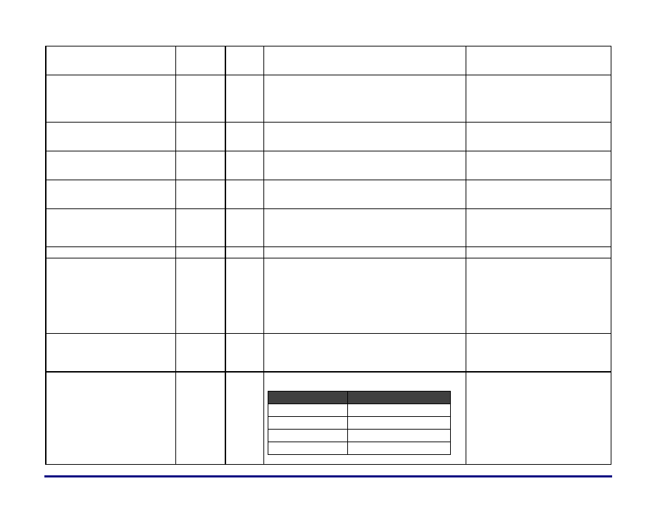
CONFIG_MODESEL[2:0]
CFG
Input
Configuration mode selection inputs to define the FPGA
configuration unit (FCU) mode of operation.
Configuration Mode
CONFIG_MODESEL[2:0]
Serial x1 Flash
001
Serial x4 Flash
010
CPU
100
JTAG
Always active
Do not leave these pins unconnected. They
should be connected to configurable inputs
like DIP switches to toggle between modes
of operation for debug. If this is not
possible or desired, based on the config
scheme, these pins should be tied to 1.8V
(VDDO_JCFG / PA_VDD2) or GND.