Ac switching characteristics – Cypress CY14E102L User Manual
Page 9
ADVANCE
CY14E102L, CY14E102N
Document Number: 001-45755 Rev. *A
Page 9 of 21
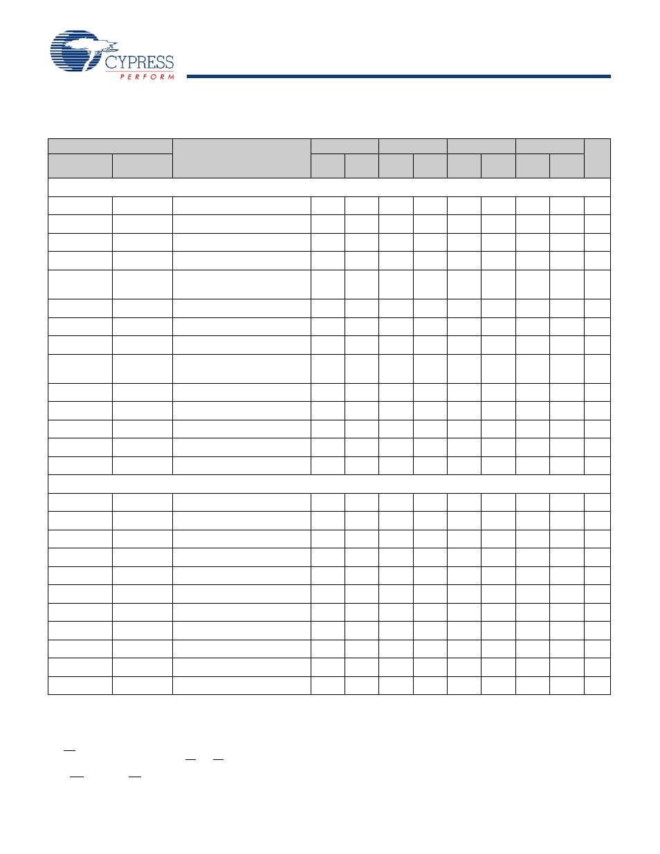
AC Switching Characteristics
The following table lists the AC switching characteristics.
Parameters
Description
15 ns
20 ns
25 ns
45 ns
Unit
Cypress
Parameters
Alt
Parameters
Min
Max
Min
Max
Min
Max
Min
Max
SRAM Read Cycle
t
ACE
t
ACS
Chip Enable Access Time
15
20
25
45
ns
t
RC
t
RC
Read Cycle Time
15
20
25
45
ns
t
AA
t
AA
Address Access Time
15
20
25
45
ns
t
DOE
t
OE
Output Enable to Data Valid
10
10
12
20
ns
t
OHA
t
OH
Output Hold After Address
Change
3
3
3
3
ns
t
LZCE
t
LZ
Chip Enable to Output Active
3
3
3
3
ns
t
HZCE
t
HZ
Chip Disable to Output Inactive
7
8
10
15
ns
t
LZOE
t
OLZ
Output Enable to Output Active
0
0
0
0
ns
t
HZOE
t
OHZ
Output Disable to Output
Inactive
7
8
10
15
ns
t
PU
t
PA
Chip Enable to Power Active
0
0
0
0
ns
t
PD
t
PS
Chip Disable to Power Standby
15
20
25
45
ns
t
DBE
-
Byte Enable to Data Valid
10
10
12
20
ns
t
LZBE
-
Byte Enable to Output Active
0
0
0
0
ns
t
HZBE
-
Byte Disable to Output Inactive
7
8
10
15
ns
SRAM Write Cycle
t
WC
t
WC
Write Cycle Time
15
20
25
45
ns
t
PWE
t
WP
Write Pulse Width
10
15
20
30
ns
t
SCE
t
CW
Chip Enable To End of Write
15
15
20
30
ns
t
SD
t
DW
Data Setup to End of Write
5
8
10
15
ns
t
HD
t
DH
Data Hold After End of Write
0
0
0
0
ns
t
AW
t
AW
Address Setup to End of Write
10
15
20
30
ns
t
SA
t
AS
Address Setup to Start of Write
0
0
0
0
ns
t
HA
t
WR
Address Hold After End of Write
0
0
0
0
ns
t
HZWE
t
WZ
Write Enable to Output Disable
7
8
10
15
ns
t
LZWE
t
OW
Output Active after End of Write
3
3
3
3
ns
t
BW
-
Byte Enable to End of Write
15
15
20
30
ns
Notes
12. WE must be HIGH during SRAM read cycles.
13. Device is continuously selected with CE and OE both LOW.
14. Measured ±200 mV from steady state output voltage.
15. If WE is LOW when CE goes LOW, the output goes into high impedance state.