Maximum ratings, Operating range, Dc electrical characteristics – Cypress STK11C68-5 User Manual
Page 5: Data retention and endurance, Capacitance
STK11C68-5 (SMD5962-92324)
Document Number: 001-51001 Rev. *A
Page 5 of 15
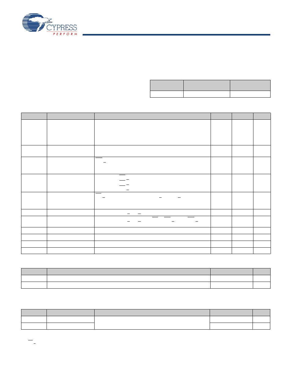
Maximum Ratings
Exceeding maximum ratings may shorten the useful life of the
device. These user guidelines are not tested.
Storage Temperature ................................. –65
°C to +150°C
Temperature under bias.............................. –55
°C to +125°C
Supply Voltage on V
CC
Relative to GND ..........–0.5V to 7.0V
Voltage on Input Relative to Vss............ –0.6V to V
CC
+ 0.5V
Voltage on DQ
0-7
...................................–0.5V to Vcc + 0.5V
Power Dissipation ......................................................... 1.0W
DC Output Current (1 output at a time, 1s duration).... 15 mA
Operating Range
Range
Ambient
Temperature
V
CC
Military
-55
°C to +125°C
4.5V to 5.5V
DC Electrical Characteristics
Over the operating range (V
CC
= 4.5V to 5.5V)
Parameter
Description
Test Conditions
Min
Max
Unit
I
CC1
Average V
CC
Current
t
RC
= 35 ns
t
RC
= 45 ns
t
RC
= 55 ns
Dependent on output loading and cycle rate. Values obtained
without output loads. I
OUT
= 0 mA
75
65
55
mA
mA
mA
I
CC2
Average V
CC
Current
during STORE
All Inputs Do Not Care, V
CC
= Max
Average current for duration t
STORE
3
mA
I
CC3
Average V
CC
Current at
t
RC
= 200 ns, 5V, 25°C
Typical
WE > (V
CC
– 0.2V). All other inputs cycling.
Dependent on output loading and cycle rate. Values obtained
without output loads.
10
mA
I
SB1
V
CC
Standby Current
(Standby, Cycling TTL
Input Levels)
t
RC
= 35 ns, CE > V
IH
t
RC
= 45 ns, CE > V
IH
t
RC
= 55 ns, CE > V
IH
24
21
20
mA
mA
mA
I
SB2
V
CC
Standby Current
CE > (V
CC
– 0.2V). All others V
IN
< 0.2V or > (V
CC
– 0.2V).
Standby current level after nonvolatile cycle is complete.
Inputs are static. f = 0 MHz
1500
μA
I
IX
Input Leakage Current
V
CC
= Max, V
SS
< V
IN
< V
CC
-1
+1
μA
I
OZ
Off State Output
Leakage Current
V
CC
= Max, V
SS
< V
IN
< V
CC
, CE or OE > V
IH
or WE < V
IL
-5
+5
μA
V
IH
Input HIGH Voltage
2.2
V
CC
+ 0.5
V
V
IL
Input LOW Voltage
V
SS
– 0.5
0.8
V
V
OH
Output HIGH Voltage
I
OUT
= –4 mA
2.4
V
V
OL
Output LOW Voltage
I
OUT
= 8 mA
0.4
V
Data Retention and Endurance
Parameter
Description
Min
Unit
DATA
R
Data Retention
100
Years
NV
C
Nonvolatile STORE Operations
1,000
K
Capacitance
In this table, the capacitance parameters are listed.
Parameter
Description
Test Conditions
Max
Unit
C
IN
Input Capacitance
T
A
= 25
°C, f = 1 MHz,
V
CC
= 0 to 3.0V
8
pF
C
OUT
Output Capacitance
7
pF
Note
2. CE > V
IH
does not produce standby current levels until any nonvolatile cycle in progress has timed out.
3. These parameters are guaranteed by design and are not tested.