Switching waveforms, Continued) – Cypress CY7C1380FV25 User Manual
Page 22

CY7C1380DV25, CY7C1380FV25
CY7C1382DV25, CY7C1382FV25
Document #: 38-05546 Rev. *E
Page 22 of 29
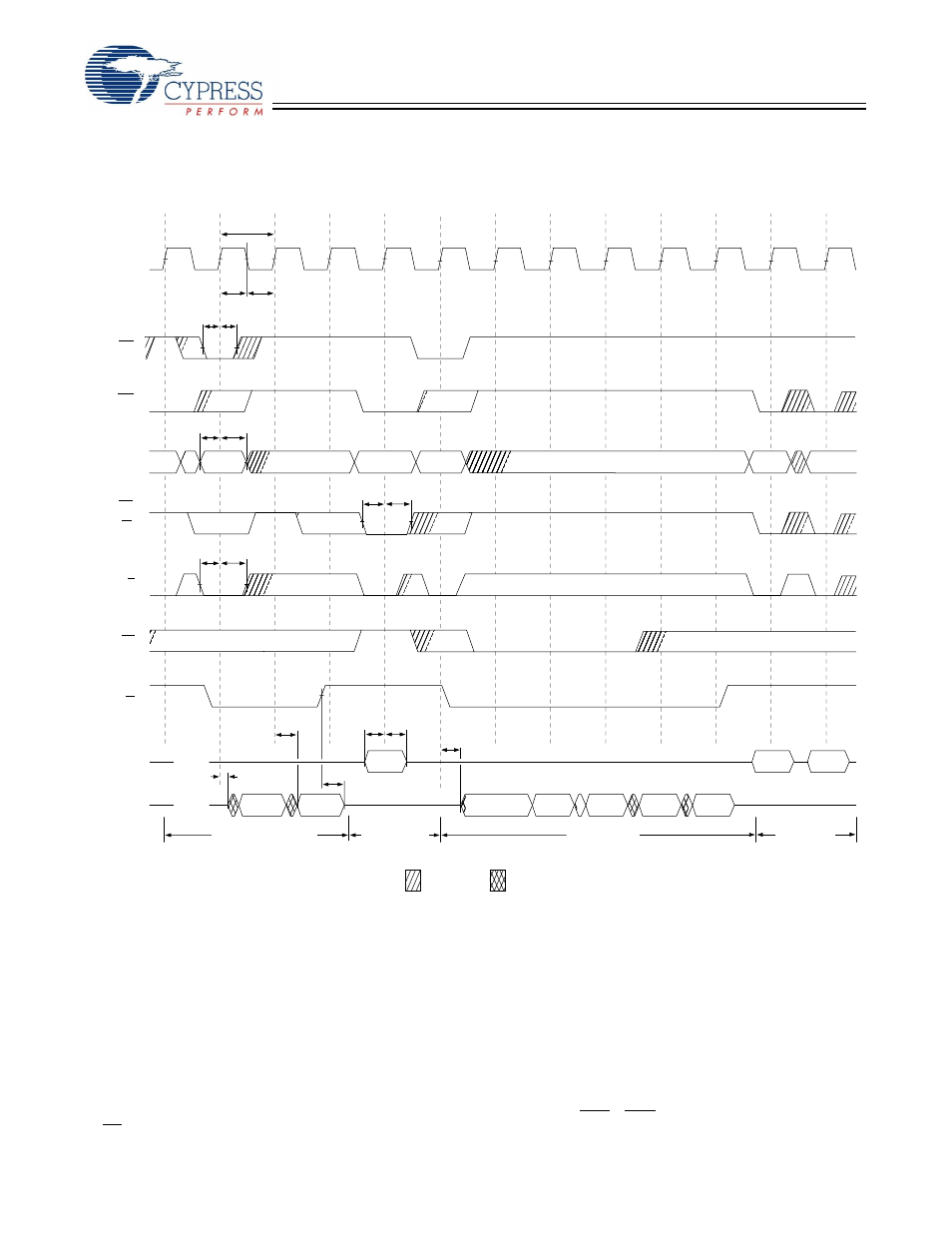
Read/Write Cycle Timing
Switching Waveforms
(continued)
tCYC
tCL
CLK
ADSP
tADH
tADS
ADDRESS
tCH
OE
ADSC
CE
tAH
tAS
A2
tCEH
tCES
BWE,
BW
X
Data Out (Q)
High-Z
ADV
Single WRITE
D(A3)
A4
A5
A6
D(A5)
D(A6)
Data In (D)
BURST READ
Back-to-Back READs
High-Z
Q(A2)
Q(A1)
Q(A4)
Q(A4+1)
Q(A4+2)
tWEH
tWES
Q(A4+3)
tOEHZ
tDH
tDS
tOELZ
tCLZ
tCO
Back-to-Back
WRITEs
A1
DON’T CARE
UNDEFINED
A3
Notes:
27. The data bus (Q) remains in high-Z following a write cycle, unless a new read access is initiated by ADSP or ADSC.
28. GW is HIGH.
This manual is related to the following products:
