Ac test loads and waveforms, Switching characteristics – Cypress CY7C1019CV33 User Manual
Page 4
CY7C1019CV33
Document #: 38-05130 Rev. *F
Page 4 of 10
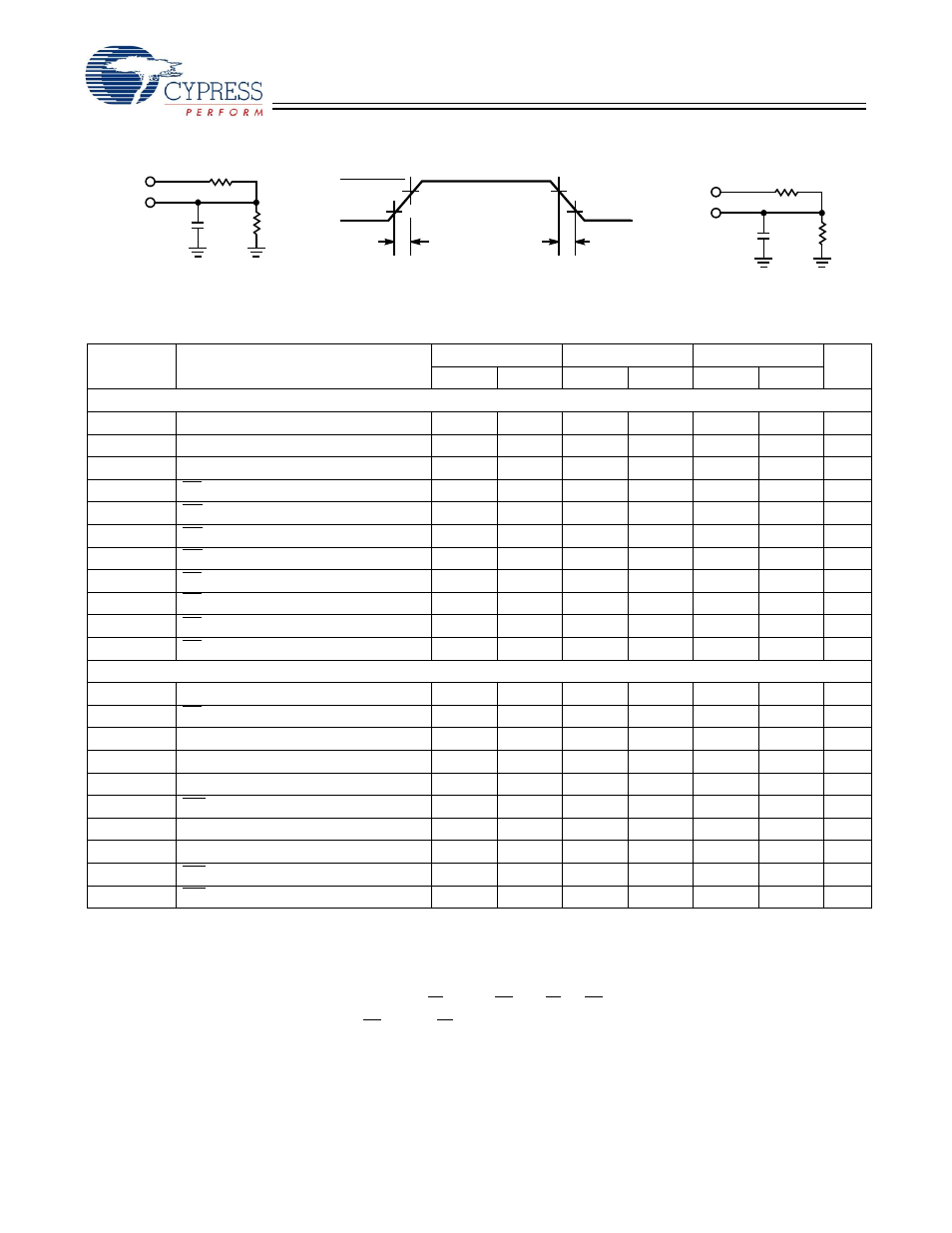
AC Test Loads and Waveforms
[4]
Switching Characteristics
Over the Operating Range
[5]
Parameter
Description
-10
-12
-15
Unit
Min.
Max.
Min.
Max.
Min.
Max.
Read Cycle
t
RC
Read Cycle Time
10
12
15
ns
t
AA
Address to Data Valid
10
12
15
ns
t
OHA
Data Hold from Address Change
3
3
3
ns
t
ACE
CE LOW to Data Valid
10
12
15
ns
t
DOE
OE LOW to Data Valid
5
6
7
ns
t
LZOE
OE LOW to Low Z
0
0
0
ns
t
HZOE
OE HIGH to High Z
[6, 7]
5
6
7
ns
t
LZCE
CE LOW to Low Z
[7]
3
3
3
ns
t
HZCE
CE HIGH to High Z
[6, 7]
5
6
7
ns
t
PU
[8]
CE LOW to Power-Up
0
0
0
ns
t
PD
[8]
CE HIGH to Power-Down
10
12
15
ns
Write Cycle
[9, 10]
t
WC
Write Cycle Time
10
12
15
ns
t
SCE
CE LOW to Write End
8
9
10
ns
t
AW
Address Set-Up to Write End
8
9
10
ns
t
HA
Address Hold from Write End
0
0
0
ns
t
SA
Address Set-Up to Write Start
0
0
0
ns
t
PWE
WE Pulse Width
7
8
10
ns
t
SD
Data Set-Up to Write End
5
6
8
ns
t
HD
Data Hold from Write End
0
0
0
ns
t
LZWE
WE HIGH to Low Z
[7]
3
3
3
ns
t
HZWE
WE LOW to High Z
[6, 7]
5
6
7
ns
Notes:
4. AC characteristics (except High-Z) for all speeds are tested using the Thevenin load shown in Figure (a). High-Z characteristics are tested for all speeds using
the test load shown in Figure (c).
5. Test conditions assume signal transition time of 3 ns or less, timing reference levels of 1.5V, input pulse levels of 0 to 3.0V.
6. t
HZOE
, t
HZCE
, and t
HZWE
are specified with a load capacitance of 5 pF as in part (d) of AC Test Loads. Transition is measured
±500 mV from steady-state voltage.
7. At any given temperature and voltage condition, t
HZCE
is less than t
LZCE
, t
HZOE
is less than t
LZOE
, and t
HZWE
is less than t
LZWE
for any given device.
8. This parameter is guaranteed by design and is not tested.
9. The internal write time of the memory is defined by the overlap of CE LOW and WE LOW. CE and WE must be LOW to initiate a write, and the transition of
any of these signals can terminate the write. The input data set-up and hold timing should be referenced to the leading edge of the signal that terminates the write.
10. The minimum write cycle time for Write Cycle no. 3 (WE controlled, OE LOW) is the sum of t
HZWE
and t
SD
.
90%
10%
3.0V
GND
90%
10%
ALL INPUT PULSES
3.3V
OUTPUT
30 pF
(a)
R 317
Ω
R2
351
Ω
Rise Time: 1 V/ns
Fall Time: 1 V/ns
(b)
3.3V
OUTPUT
5 pF
(c)
R 317
Ω
R2
351
Ω
High-Z characteristics: