Cypress CY7C1019CV33 User Manual
128k x 8 static ram, Features, Functional description
128K x 8 Static RAM
CY7C1019CV33
Cypress Semiconductor Corporation
•
198 Champion Court
•
San Jose
,
CA 95134-1709
•
408-943-2600
Document #: 38-05130 Rev. *F
Revised August 3, 2006
Features
• Pin and function compatible with CY7C1019BV33
• High speed
— t
AA
= 10 ns
• CMOS for optimum speed/power
• Data retention at 2.0V
• Center power/ground pinout
• Automatic power-down when deselected
• Easy memory expansion with CE
and OE options
• Available in Pb-free and non Pb-free 48-ball VFBGA,
32-pin TSOP II and 400-mil SOJ package
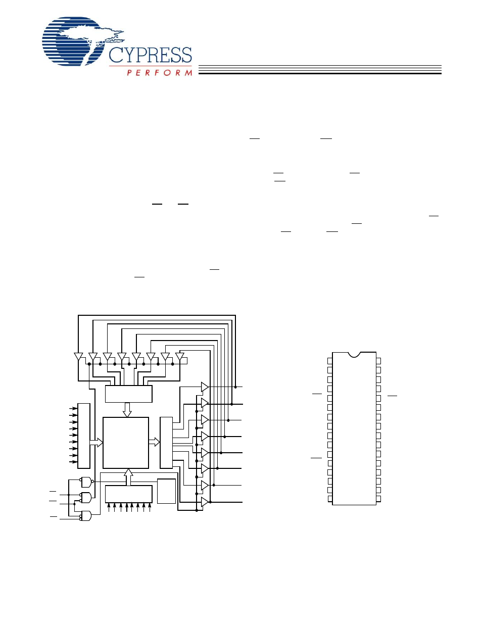
Functional Description
The CY7C1019CV33 is a high-performance CMOS static
RAM organized as 131,072 words by 8 bits. Easy memory
expansion is provided by an active LOW Chip Enable (CE), an
active LOW Output Enable (OE), and tri-state drivers. This
device has an automatic power-down feature that significantly
reduces power consumption when deselected.
Writing to the device is accomplished by taking Chip Enable
(CE) and Write Enable (WE) inputs LOW. Data on the eight I/O
pins (I/O
0
through I/O
7
) is then written into the location
specified on the address pins (A
0
through A
16
).
Reading from the device is accomplished by taking Chip
Enable (CE) and Output Enable (OE) LOW while forcing Write
Enable (WE) HIGH. Under these conditions, the contents of
the memory location specified by the address pins will appear
on the I/O pins.
The eight input/output pins (I/O
0
through I/O
7
) are placed in a
high-impedance state when the device is deselected (CE
HIGH), the outputs are disabled (OE HIGH), or during a write
operation (CE LOW, and WE LOW).
The CY7C1019CV33 is available in Standard 48-ball FBGA,
32-pin TSOP II and 400-mil-wide SOJ packages
14
15
Logic Block Diagram
Pin Configuration
A
1
A
2
A
3
A
4
A
5
A
6
A
7
A
8
COLUMN
DECODER
RO
W
D
E
CO
D
E
R
SE
NSE AM
PS
INPUT BUFFER
POWER
DOWN
WE
OE
I/O
0
I/O
1
I/O
2
I/O
3
128K x 8
ARRAY
I/O
7
I/O
6
I/O
5
I/O
4
A
0
A
11
A
13
A
12
A
A
10
CE
A
A
16
A
9
1
2
3
4
5
6
7
8
9
10
11
14
19
20
24
23
22
21
25
28
27
26
Top View
SOJ/TSOP II
12
13
29
32
31
30
16
15
17
18
A
7
A
1
A
2
A
3
CE
I/O
0
I/O
1
V
CC
A
13
A
16
A
15
OE
I/O
7
I/O
6
A
12
A
11
A
10
A
9
I/O
2
A
0
A
4
A
5
A
6
I/O
4
V
CC
I/O
5
A
8
I/O
3
WE
V
SS
A
14
V
SS