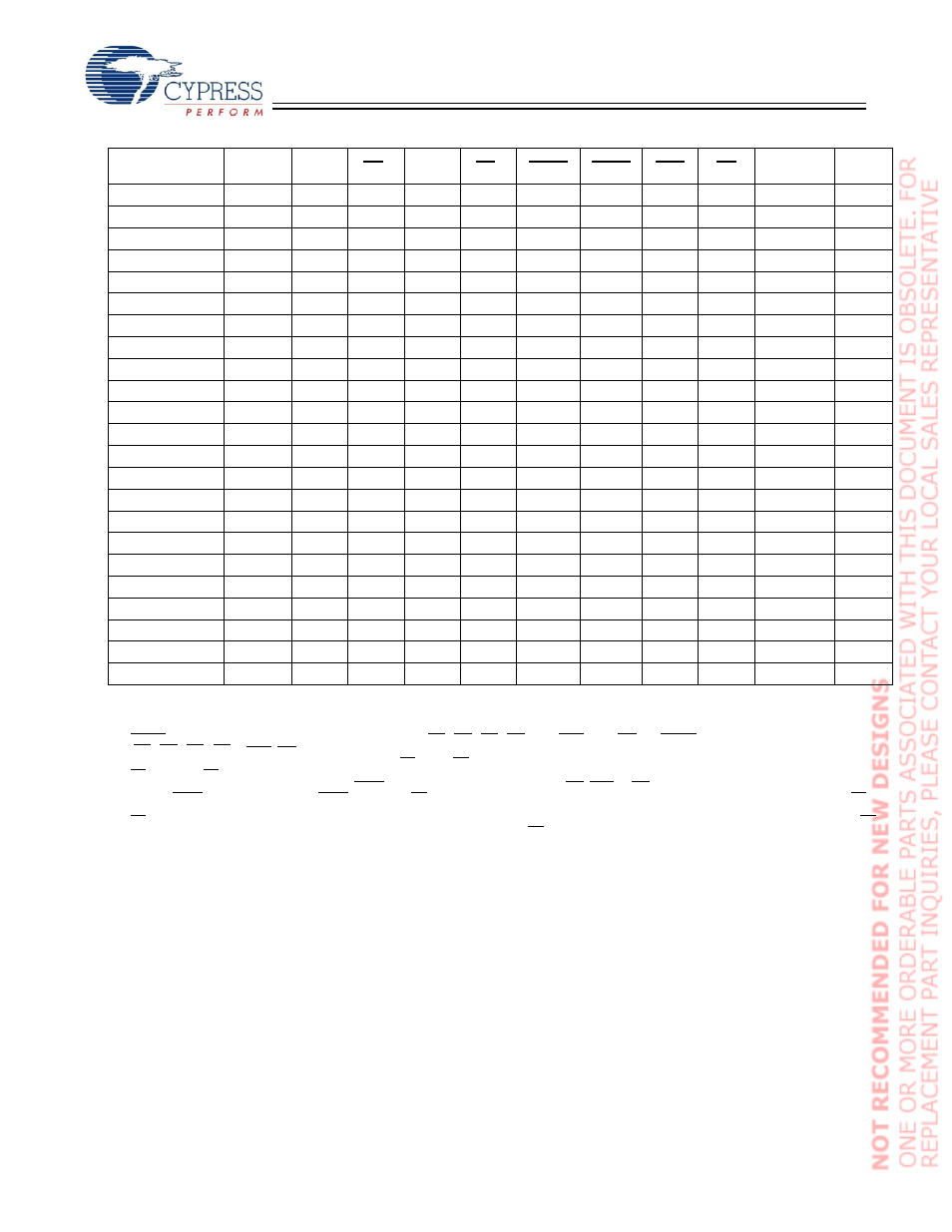
Truth table – Cypress CY7C1364C User Manual
Page 7
CY7C1364C
Document #: 38-05689 Rev. *E
Page 7 of 18
Truth Table
[3, 4, 5, 6, 7, 8]
Next Cycle
Address
Used
ZZ
CE
3
CE
2
CE
1
ADSP
ADSC
ADV
OE
DQ
Write
Unselected
None
L
X
X
H
X
L
X
X
Tri-State
X
Unselected
None
L
H
X
L
L
X
X
X
Tri-State
X
Unselected
None
L
X
L
L
L
X
X
X
Tri-State
X
Unselected
None
L
H
X
L
H
L
X
X
Tri-State
X
Unselected
None
L
X
L
L
H
L
X
X
Tri-State
X
Begin Read
External
L
L
H
L
L
X
X
X
Tri-State
X
Begin Read
External
L
L
H
L
H
L
X
X
Tri-State
Read
Continue Read
Next
L
X
X
X
H
H
L
H
Tri-State
Read
Continue Read
Next
L
X
X
X
H
H
L
L
DQ
Read
Continue Read
Next
L
X
X
H
X
H
L
H
Tri-State
Read
Continue Read
Next
L
X
X
H
X
H
L
L
DQ
Read
Suspend Read
Current
L
X
X
X
H
H
H
H
Tri-State
Read
Suspend Read
Current
L
X
X
X
H
H
H
L
DQ
Read
Suspend Read
Current
L
X
X
H
X
H
H
H
Tri-State
Read
Suspend Read
Current
L
X
X
H
X
H
H
L
DQ
Read
Begin Write
Current
L
X
X
X
H
H
H
X
Tri-State
Write
Begin Write
Current
L
X
X
H
X
H
H
X
Tri-State
Write
Begin Write
External
L
L
H
L
H
H
X
X
Tri-State
Write
Continue Write
Next
L
X
X
X
H
H
H
X
Tri-State
Write
Continue Write
Next
L
X
X
H
X
H
H
X
Tri-State
Write
Suspend Write
Current
L
X
X
X
H
H
H
X
Tri-State
Write
Suspend Write
Current
L
X
X
H
X
H
H
X
Tri-State
Write
ZZ “Sleep”
None
H
X
X
X
X
X
X
X
Tri-State
X
Notes:
3. X = “Don't Care.” H = Logic HIGH, L = Logic LOW.
4. WRITE = L when any one or more Byte Write Enable signals (BW
A
,BW
B
,BW
C
,BW
D
) and BWE = L or GW = L. WRITE = H when all Byte Write Enable signals
(BW
A
,BW
B
,BW
C
,BW
D
), BWE, GW = H.
5. The DQ pins are controlled by the current cycle and the OE signal. OE is asynchronous and is not sampled with the clock.
6. CE
1
, CE
2
, and CE
3
are available only in the TQFP package.
7. The SRAM always initiates a Read cycle when ADSP is asserted, regardless of the state of GW, BWE, or BW
[A:D]
. Writes may occur only on subsequent clocks
after the ADSP or with the assertion of ADSC. As a result, OE must be driven HIGH prior to the start of the Write cycle to allow the outputs to tri-state. OE is a
don't care for the remainder of the Write cycle.
8. OE is asynchronous and is not sampled with the clock rise. It is masked internally during Write cycles. During a Read cycle all data bits are tri-state when OE is
inactive or when the device is deselected, and all data bits behave as output when OE is active (LOW).