Output channel diagnostics, Figure 4 simplified driver circuit diagram, Trusted – Rockwell Automation T8480 Trusted TMR Analogue Output Module - 40 Channel User Manual
Page 14: Module t8480, For an un-faulted transistor
Trusted
TM
Module T8480
Issue 13 Apr 10
PD-T8480
14
Note: In this context, N.O. is defined as being in the off state in the absence of control signal power,
and similarly, N.C. is the on state in the absence of control signal power. These switches are
constructed from enhancement mode MOSFETs and are both guaranteed to be off in the
absence of module power to create gate voltage signals to bias them on
(unlike
electromechanical relays for example).
The reason that the lower switches are specified to be on in the absence of control signal power is to
allow two channels to power the load should an entire slice fail. Even if an entire slice fails, the
surviving output circuits will carry the necessary control. The structure of each OFIU output driver is
shown below:
UPSTREAM
ENABLE
R
S
LO
A
D
ADC
PRM
5V
24V V
FIELD
OPTO
COMMAND
POWER
OPTO
RESPONSE
FPGA
GFSS
DOWNSTREAM
ENABLE
C
F
R
F
F
R
O
M
H
IU
F
R
O
M
U
P
S
T
R
E
A
M
S
L
IC
E
I
L
O
A
D
I
F
E
T
I
V
S
E
N
S
E
TOP_RAIL
FET 1
FET 2
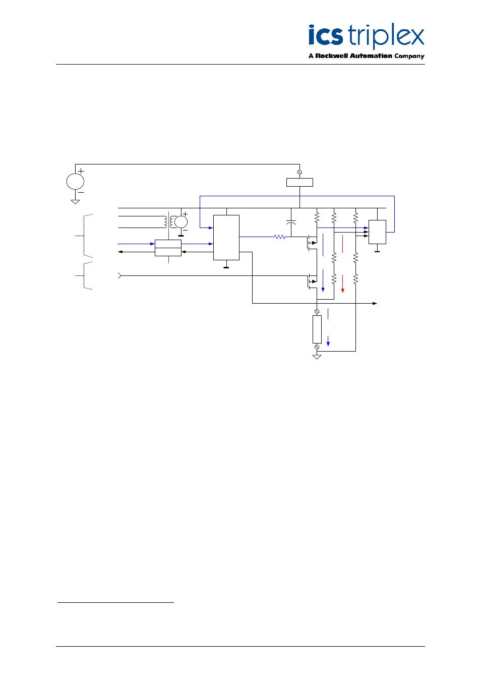
Figure 4 Simplified Driver Circuit Diagram
A sense resistor provides a means of continuously monitoring the output current, as measured with an
A/D channel. Closed loop control logic in the FPGA provides a Pulse-Ratio-Modulated drive signal to
the gate of FET 1 to maintain a constant current equal to the commanded output, based on the A/D
feedback.
A level translator transistor is used to drive the gate of FET 2. It provides FET 2 with a negative gate
voltage, to minimize its on resistance, and serves to hold FET 2 on in the event that the secondary gate
control loses power.
1.9.1. Output Channel Diagnostics
The measured output channel current is continuously monitored relative to the commanded output
current, and compared to the current reported from each independent slice. In the event that there is a
discrepancy that falls outside the authority of the control loop to overcome, then remedial action is
engaged which disables FET 2 for the affected slice and causes the surviving slices to compensate in
order to maintain the commanded current to the load.
The voltage across the load is also measured by each slice, and continuously compared for equality. If
there is a discrepancy between the slices, then the discrepant slice is removed from service, and the
survivors compensate to maintain the commanded current to the load.
Each channel is continuously monitored to determine the presence of field faults, such as an open
circuit, or lack of field loop power.
3
For an un-faulted transistor.