14 digital signal connections, 15 los indicators, 16 jtag connection – Cirrus Logic CDB61884 User Manual
Page 9: 17 host interface connection, Host setup description, Host software interface, Host setup description 4. host software interface, Figure 10. digital signal control/access, Table 3. switch settings for host mode

CDB61884
DS485DB1
9
in the open “HIGH” position selects multiplex and
the closed “LOW” position selects Non-multiplex
2.14
Digital Signal Connections
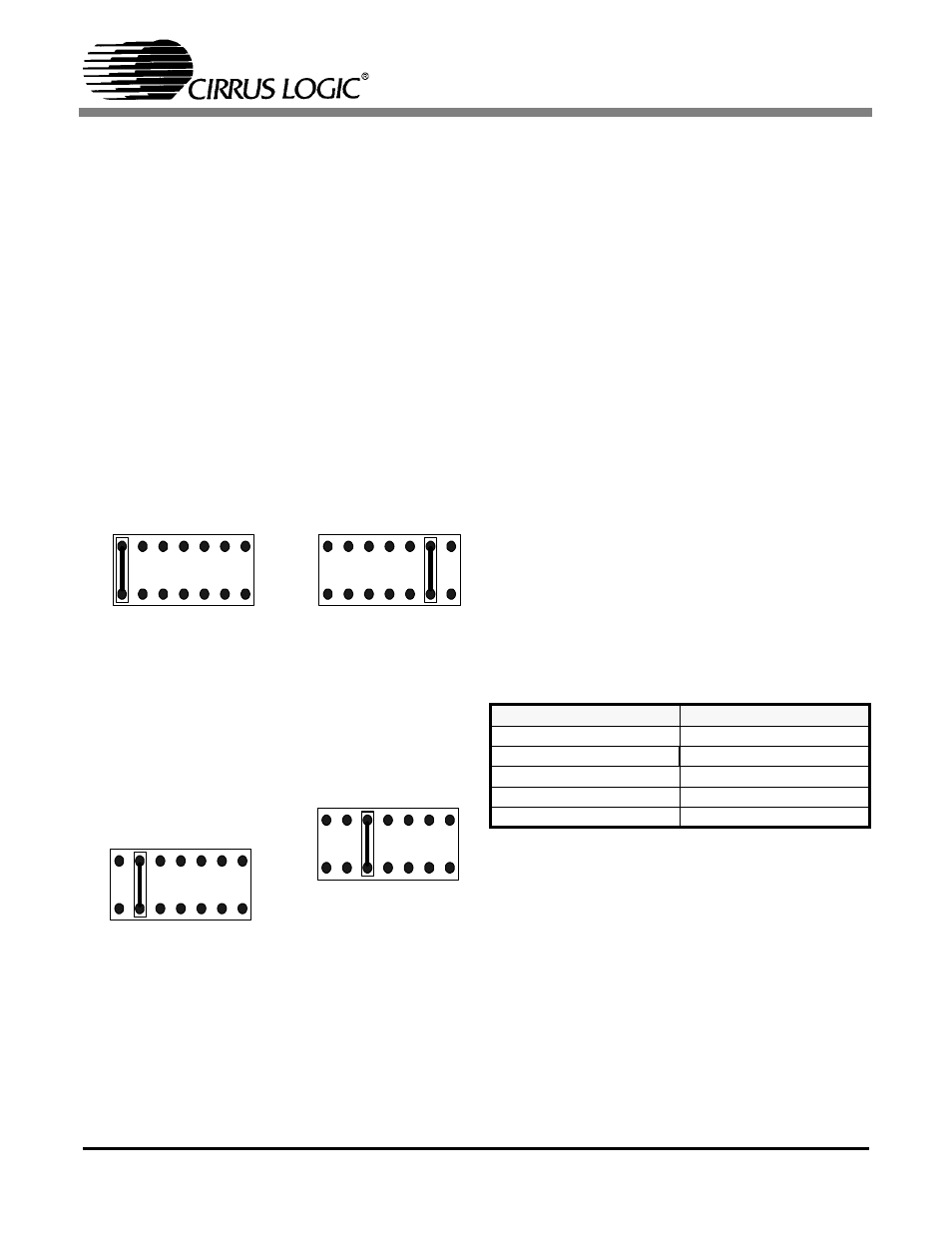
There are eight fourteen pin bed stake headers (la-
beled J4 through J11) that provide access to the
digital signals used to interface with back-end de-
vices (framers, mappers, ASIC, etc.) and all eight
LOS signals, in both hardware and host mode.
shows the layout for one of the eight 14-
pin bed stake headers used to access the back-end
digital signals, LOS signals and the different set-
tings for the TCLK/TNEG pins.
2.15
LOS Indicators
The two 4-LED packs D1 and D2 (labeled ALOS
0-7) represent the LOS signal status for LOS 0-7
pins. The ALOS 0-7 LEDs will illuminate when the
corresponding receiver has detected a loss of signal
condition. Refer to the CS61884 Data Sheet for
LOS conditions.
2.16
JTAG Connection
A 5-pin bed stake header (J60) is provided to allow
easy access to the IEEE 1149.1 JTAG Boundary
Scan signals from the device.
2.17
Host Interface Connection
Connector J12 is used to connect the CS61884
evaluation board to the host computer, through a
standard 25 pin male to female parallel port cable.
No external
µ
Controller board is required for host
interface connection. This connector is used for
both serial and parallel interface.
3. HOST SETUP DESCRIPTION
Place the switches shown in Table 3 to the stated
configuration before setting the Mode switch (S15)
to Serial or Parallel host mode. Refer to the
for switch S15 settings.
– Switches #1 and #2 inside of switch block S9
are used in parallel host mode to select
Motorola, Intel, multiplex or Non-multiplex
modes. Switch S9 #1 and #2 are not used in
Serial host mode.
4. HOST SOFTWARE INTERFACE
The software provided with the CDB61884 evalu-
ation board is used to control and monitor the
CS61884 device. The program is designed to auto-
matically read back each bit after each write. If the
bit is read back incorrectly an error will occur. The
J1
TC
L
K
#
TC
L
K
#
TC
L
K
#
TP
O
S
#
TN
E
G
#
TN
E
G
#
LOS
#
RCL
K
#
GN
D
RP
O
S
#
RNE
G
#
V
logi
c
GN
D
J1
TC
L
K
#
TC
L
K
#
TC
L
K
#
TP
O
S
#
TN
E
G
#
TN
E
G
#
LOS
#
RCL
K
#
GN
D
RP
O
S
#
RNE
G
#
V
logi
c
GN
D
J1
TC
L
K
#
TC
L
K
#
TC
L
K
#
TP
O
S
#
TN
E
G
#
TN
E
G
#
LOS
#
RCL
K
#
GN
D
RP
O
S
#
RNE
G
#
V
logi
c
GN
D
Bi-polar Mode
TAOS active when
MCLK present
RZ mode active when
MCLK absent
J1
TC
L
K
#
TC
L
K
#
TC
L
K
#
TP
O
S
#
TN
E
G
#
TN
E
G
#
LOS
#
RCL
K
#
GN
D
RP
O
S
#
RNE
G
#
V
logi
c
GN
D
Transmitters High-Z
Uni-Polar Mode Active
V
logi
c
V
logi
c
V
logi
c
V
logi
c
Figure 10. Digital Signal Control/Access
Table 3. Switch Settings for Host Mode
Switch
Position
S1 through S8
NONE (middle)
S9 # 3 through # 7
OPEN (low)
S10
OPEN (middle)
S11
NC (middle)
S12 through S14
OPEN (middle)
