Board component descriptions, 1 power connections, 2 master clock selection – Cirrus Logic CDB61884 User Manual
Page 5: 1 power connections 2.2 master clock selection, Board component descriptions 2.1 power connections, Figure 2. on-board logic power selection, Figure 3. master clock selections
CDB61884
DS485DB1
5
2. BOARD COMPONENT DESCRIPTIONS
2.1
Power Connections
Power for the evaluation board is supplied by an
external +3.3 V DC power supply. A +5 V DC
power supply can also be connected to the on-board
control logic. The LED labeled “D3” will illumi-
nate when power is supplied to the on-board con-
trol logic.
– Connect the +3.3 VDC power supply to the +3V
binding post and the +5 VDC power supply to
the +5 V binding post if 5 Volt logic is required
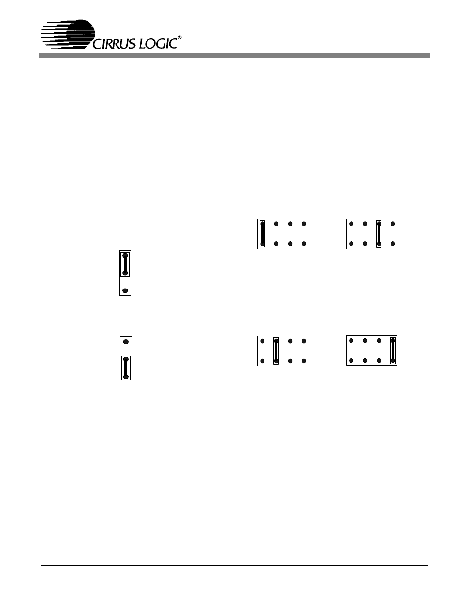
– Jumper J13 shown in
allows all the
external logic on the evaluation board to be
connected to either +3 V or +5 V binding post.
– To measure the current consumption of only
the CS61884 device, place a short block on
Jumper J13 to connect the Vlogic power
supplies to the +5 V binding post. This will
isolate the CS61884 device from all the on-
board logic, to allow the current measurement
to be made at the +3 V binding post.
2.2
Master Clock Selection
In both hardware and host modes, the MCLK pin is
configured by placing a short block on one of the
positions of bed stake header J1.
shows
the different positions of the J1 bed stake header.
– A 2.048 MHz clock oscillator is provided on the
evaluation board for use as the on-board clock
source for all E1 modes.
– A 1.544 MHz clock oscillator is also provided
with the evaluation board for use as the on-
board clock source for the T1/J1 operation
modes.
– A BNC connector (labeled J16) provides the
connection for an external clock source.
J 1 3
3 V
5 V
O n -b o a rd lo g ic c o n n e c te d
to + 3 V b in d in g p o s t
O n -b o a rd lo g ic c o n n e c te d
to + 5 V b in d in g p o s t
V L O G IC
J 1 3
3 V
5 V
V L O G IC
Figure 2. On-board Logic Power Selection
MCLK
J1
Data Recovery Mode
EXT
E
RNAL
S
OURCE
HI
GH
O
S
C
ILLATO
R
GND
MCLK
J1
External Clock Source
HI
GH
O
S
C
ILLATO
R
GND
J1
Receivers Powered Down
HI
GH
O
S
C
ILLATO
R
GND
J1
HI
GH
O
S
C
ILLATO
R
GND
On-board Oscillator
MCLK
MCLK
EXT
E
RNAL
S
OURCE
EXT
ERNAL
S
OURCE
EXT
ERNAL
S
OURCE
Figure 3. Master Clock Selections