6 clock edge selection, 7 jitter attenuator selection, 8 loopback mode selection – Cirrus Logic CDB61884 User Manual
Page 7: 9 line length selection
CDB61884
DS485DB1
7
mitters in a high impedance state. Removing the
shorting block, enables the transmitters.
See
2.6
Clock Edge Selection
In clock/data recovery mode, jumper J93 selects
the edge of RCLK and SCLK on which the
RPOS/RDATA, RNEG, and SDO data signals are
valid. When in data recovery mode, jumper J93 se-
lects the output polarity of RPOS/RNEG. The func-
tion of J93 applies to both the hardware and host
mode.
shows the settings for jumper J93
and the effect in both clock/data recovery and data
recovery only mode.
2.7
Jitter Attenuator Selection
In hardware mode, switch S10 (JASEL) controls
the position of the jitter attenuator for all eight
channels. The corner frequency and FIFO length
can not be changed in hardware mode.
shows the settings for switch S10.
In host mode, switch S10 has no effect on the
CS61884 device and should be set to the open
(middle) position.
2.8
Loopback Mode Selection
In hardware mode, the Loopback modes are config-
ured with switches S1 through S8 (0-7).
shows the three different settings for all eight loop
back switches.
In host mode, switches S1 through S8 must be set
to the NONE (middle) position to allow host inter-
face control.
2.9
Line Length Selection
In hardware mode, the transmit pulse shapes for E1
75
Ω
, E1 120
Ω
and T1(J1) 100
Ω
are selected with
switches S12 through S14 (LEN 2-0). Refer to the
CS61884 Data Sheet for the correct settings.
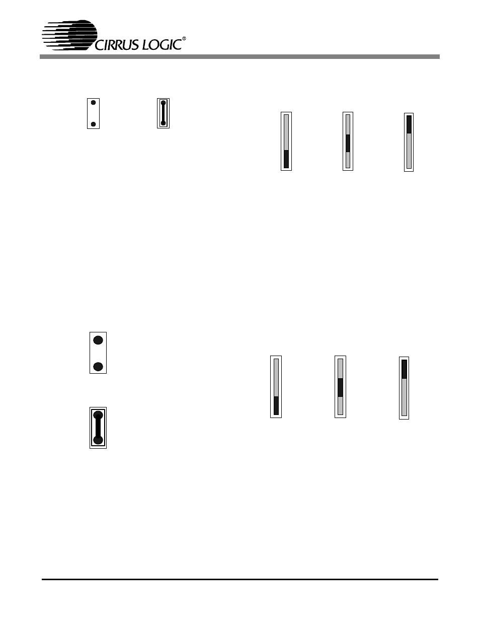
H I
LO
E nable all eight
transm itters
H i-Z all
eig ht transm itte rs
J2
3
TXO
E
HI
LO
TXO
E
J2
3
Figure 5. Transmitter Enable Selection
J9
3
HI
LO
Clock/Data Recovery -
RPOS/RNEG = falling
edge RCLK SDO =
rising edge SCLK
Clock/Data Recovery -
RPOS/RNEG = rising
edge RCLK SDO =
falling edge SCLK
Data Recovery -
RPOS/RNEG
polarity active high
Data Recovery -
RPOS/RNEG
polarity active low
CKL
E
J9
3
HI
LO
CKL
E
Figure 6. Clock Edge Selection
S10
Hardware Mode
- JA placed in
transmit path
S10
S10
HIGH
OPEN
LOW
HIGH
OPEN
LOW
HIGH
OPEN
LOW
Hardware Mode
- JA Disabled
Hardware Mode
- JA placed in
receive path
JASEL
JASEL
JASEL
Figure 7. Jitter Attenuator Selection
Hardware Mode -
Selects Remote
Loopback
Hardware Mode -
Selects local
Loopback
Hardware Mode -
Selects no
Loopback
0 - 7
0 - 7
0 - 7
S1 - S8
S1 - S8
S1 - S8
Lloop
none
Rloop
Lloop
none
Rloop
Lloop
none
Rloop
Figure 8. Loopback Mode Selection